Look down image sensor package

a technology of image sensor and package, applied in the field of package of electronic components, can solve the problem of relative thickness of image sensor assembly, and achieve the effect of reducing the overall height of the image sensor assembly and different thermal expansion coefficients

Inactive Publication Date: 2005-03-10
AMKOR TECH INC
View PDF37 Cites 61 Cited by
  • Summary
  • Abstract
  • Description
  • Claims
  • Application Information

AI Technical Summary

Benefits of technology

[0008] Further, the underfill contacts and protects the first surface of the image sensor including the active area. Thus, the underfill protects the active area against external moisture, dust and contamination. During use, electromagnetic radiation passes through the transparent substrate, through the underfill, which is transparent, and strikes the active area.
[0009] In accordance with an alternative embodiment of the present invention, an image sensor assembly includes a system board having an image sensor aperture. The image sensor assembly further includes a transparent substrate coupled to the system board and an image sensor coupled to the transparent substrate and located within the image sensor aperture. The image sensor includes a first surface facing towards the transparent substrate, the first surface having an active area. By locating the image sensor within the image sensor aperture of the system board, the overall height of the image sensor assembly is minimized.
[0013] The package body maximizes the reliability of the image sensor package by minimizing the possibility of failure of the bump and the associated dismounting of the image sensor from the transparent substrate. Further, the package body maximizes the reliability of the image sensor package by forming a redundant seal between the image sensor and the transparent substrate. In particular, the bead forms a first seal and the package body forms a second seal, which collectively protect the active area of the image sensor.

Problems solved by technology

Disadvantageously, this housing was relatively bulky and extended upwards from the printed circuit mother board or other substrate a significant distance resulting in a relatively thick image sensor assembly.

Method used


Image

  • Look down image sensor package
  • Look down image sensor package
  • Look down image sensor package

Examples


Embodiment Construction

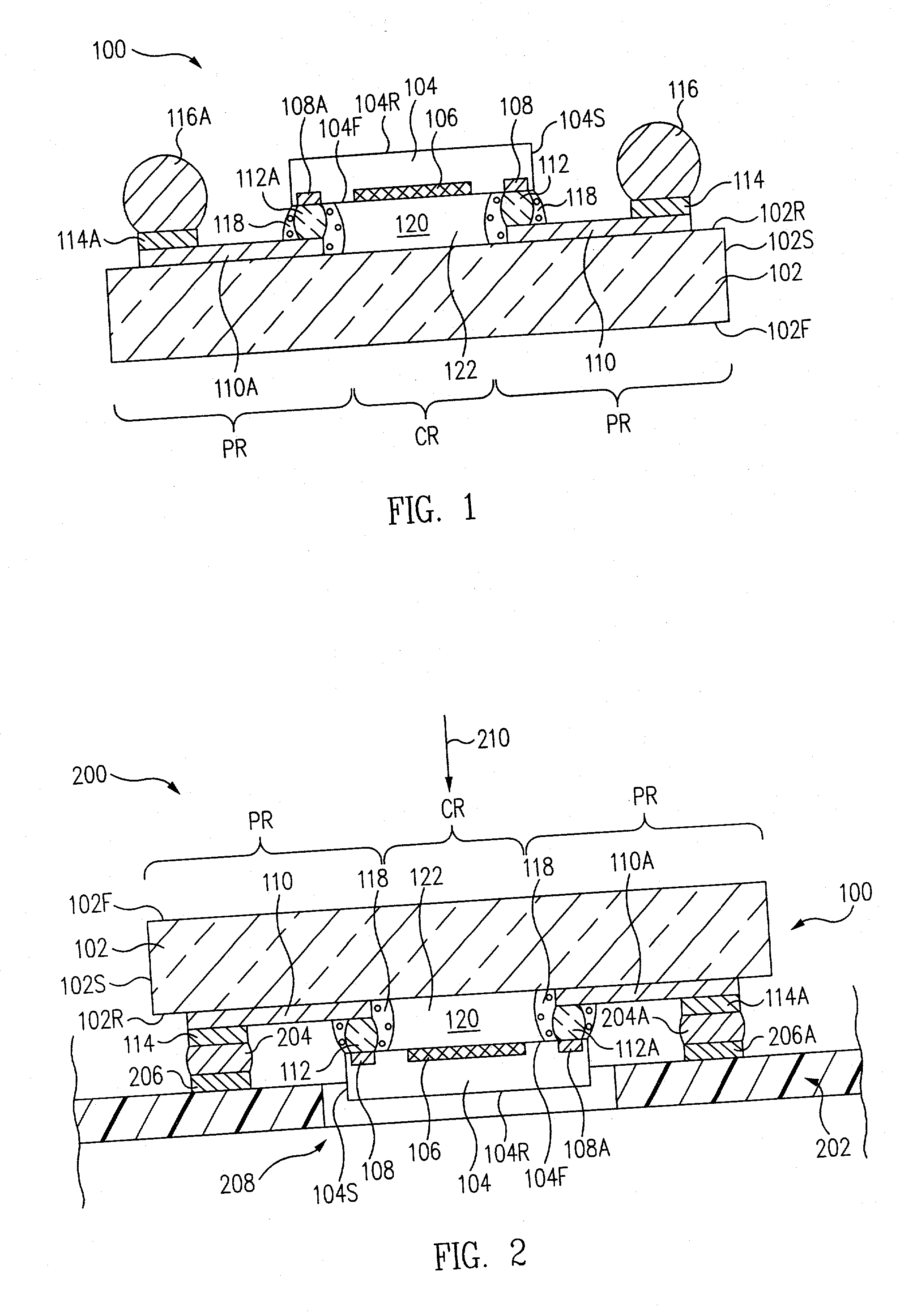
[0033]FIG. 1 is a cross-sectional view of an image sensor package 100 in accordance with one embodiment of the present invention. Image sensor package 100 includes a substrate 102 and an image sensor 104 mounted to substrate 102. Image sensor 104 includes an active area 106 on a front, e.g., first, surface 104F of image sensor 104, which faces towards substrate 102.

[0034] Generally, active area 106 is responsive to electromagnetic radiation, as is well known to those of skill in the art. For example, active area 106 is responsive to infrared radiation, ultraviolet light, and / or visible light. Illustratively, image sensor 104 is a CMOS image sensor device, a charge coupled device (CCD), or a pyroelectric device although other image sensors are used in other embodiments.

[0035] Generally, substrate 102 is transparent. In one embodiment, transparent means having a transparency sufficient for the proper operation of image sensor 104 to the electromagnetic radiation to which active area...


PUM


Abstract

An image sensor package includes a transparent substrate having an image sensor pocket. An image sensor is flip chip mounted to the transparent substrate such that the image sensor is located within the image sensor pocket. Since the image sensor is located within the image sensor pocket, the image sensor package is approximately the same thickness as the transparent substrate.

Description

BACKGROUND OF THE INVENTION [0001] 1. Field of the Invention [0002] The present invention relates generally to the packaging of electronic components. More particularly, the present invention relates to an image sensor package and method of fabricating the same. [0003] 2. Description of the Related Art [0004] Image sensors and assemblies are well known to those of skill in the art. In one conventional image sensor assembly, an image sensor was mounted to a printed circuit mother board or other substrate. After the image sensor was mounted, a housing was mounted around the image sensor and to the printed circuit mother board or other substrate. This housing provided a protective barrier around the image sensor, while at the same time, supported a window above the image sensor. During use, electromagnetic radiation passed through the window and struck the image sensor, which responded to the electromagnetic radiation. [0005] As the art moved to smaller and lighter weight electronic de...

Claims


Application Information

Patent Timeline
Patent Type & Authority Applications(United States)
IPC IPC(8): H01L27/146H01L31/0203
CPCH01L27/14618H01L31/0203H01L2224/32225H01L2224/16225H01L2224/73204H01L2924/00H01L2224/05571H01L2224/05573H01L2924/00014H01L2224/05599
Inventor HOFFMAN, PAUL ROBERT
Owner AMKOR TECH INC
Why Eureka
Try Eureka