Image-sensing apparatus

a technology of image sensor and sensor body, which is applied in the field of image sensor, can solve the problems of flat blackness, inability to acquire the data of dim parts of the subject, and inability to acquire the data of parts of the subj

Active Publication Date: 2005-03-10
SONY SEMICON SOLUTIONS CORP
View PDF1 Cites 41 Cited by
  • Summary
  • Abstract
  • Description
  • Claims
  • Application Information

AI Technical Summary

Benefits of technology

[0016] This image-sensing apparatus configured as described above permits high-quality images to be shot in accordance with the brightness of a subject by bringing the solid-state image-sensing device, for example, into the first state when the subject is dimly lit and into the second state when the subject is brightly lit.

Problems solved by technology

Accordingly, when the brightness of a subject is high, as in a case where the subject is in direct sunlight, the brightness of bright parts of the subject exceeds the level that the photosensitive devices can handle, and thus causes an overflow in them.
This makes it impossible to acquire the data of parts of the subject where the brightness exceeds that level, and thereby causes saturation.
Saturation can be avoided by shifting the brightness range in which data acquisition is feasible into a brighter region to make it possible to acquire the data of bright parts of the subject; however, this in turn makes it impossible to acquire the data of dim parts of the subject, and thus leads to flat blackness.
Therefore, using a LOG sensor tends to result in poor gradation in bright parts of a subject Accordingly, for example, whereas a LOG sensor permits acquisition of both dim and bright parts of a brightly-lit subject, it yields rather poor gradation in bright parts of a dimly-lit subject.

Method used


Image

  • Image-sensing apparatus
  • Image-sensing apparatus
  • Image-sensing apparatus

Examples


first embodiment

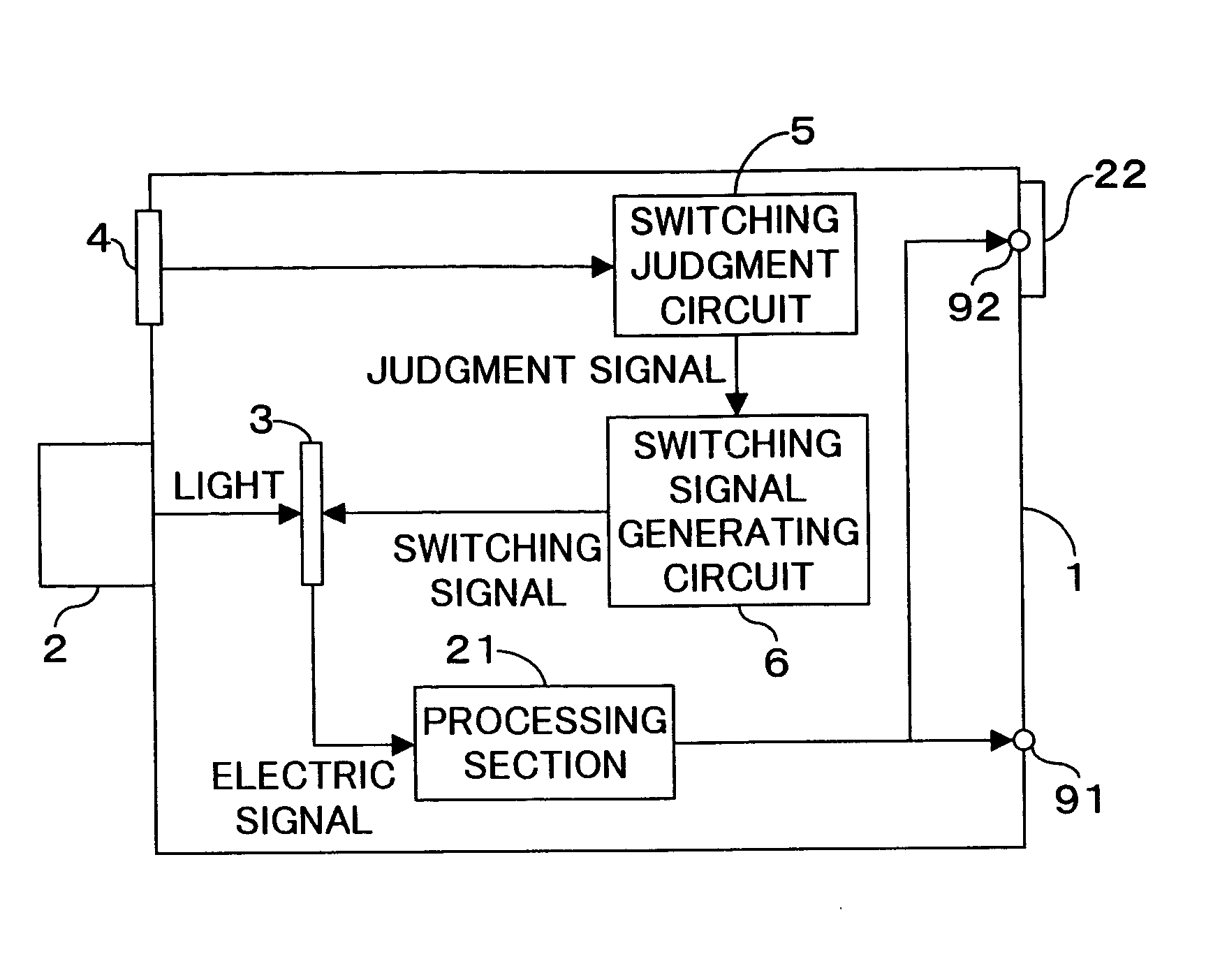
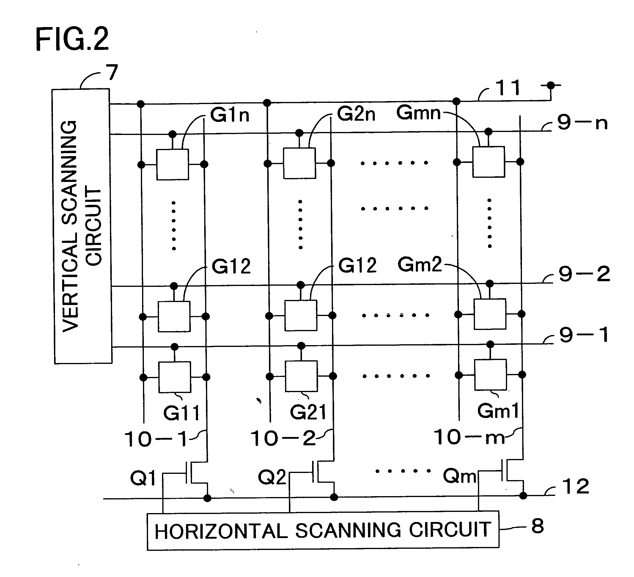
[0054] A first embodiment of the present invention will be described below with reference to the relevant drawings. FIG. 1 is a block diagram showing the internal structure of the image-sensing apparatus of a first embodiment of the invention. FIGS. 2 and 4 are block diagrams showing examples of the structure of the area sensor used as a solid-state image-sensing device in the image-sensing apparatus shown in FIG. 1. FIG. 3 is a circuit diagram showing an example of the circuit configuration of each pixel of the area sensor shown in FIG. 2. FIG. 6 is a circuit diagram showing an example of the circuit configuration of each pixel of the area sensor shown in FIG. 4.

[0055] In FIG. 1, the image-sensing apparatus 1 has an area sensor 3 that outputs an electric signal obtained by logarithmically or linearly converting the light incident thereon through an objective lens 2, a detector 4 for detecting the brightness of a subject, a switching judgment circuit 5 that determines whether to sw...

second embodiment

[0098] A second embodiment of the present invention will be described below with reference to the relevant drawings. FIG. 8 is a block diagram showing the configuration of a principal portion of the image-sensing apparatus of this embodiment. It is to be noted that, in the image-sensing apparatus shown in FIG. 8, such elements as are used for the same purposes here as in the image-sensing apparatus shown in FIG. 1 are identified with the same reference symbols, and their detailed descriptions will be omitted. In this embodiment, the area sensor and its pixels are configured in the same manner as in the first embodiment.

[0099] The image-sensing apparatus 1A shown in FIG. 8 has an objective lens 2, an area sensor 3, a switching signal generating circuit 6, a processing section 21, an automatic sensitivity adjustment circuit 40 that detects the brightness of a subject and performs sensitivity adjustment on the basis of an electric signal (brightness signal) that it receives from the a...

third embodiment

[0110] A third embodiment of the present invention will be described with reference to the relevant drawings. FIG. 11 is a block diagram showing the internal structure of the image-sensing apparatus of this embodiment. It is to be noted that, in the image-sensing apparatus shown in FIG. 11, such elements as are used for the same purposes here as in the image-sensing apparatus shown in FIG. 8 are identified with the same reference symbols, and their detailed descriptions will be omitted. In this embodiment, the area sensor and its pixels are configured in the same manner as in the first embodiment.

[0111] In the image-sensing apparatus 1B shown in FIG. 11, the switching judgment circuit 5B receives image data from the area sensor 3 instead of receiving a brightness signal as is fed to both the switching judgment circuit 5A and the automatic sensitivity adjustment circuit 40 in FIG. 8. Moreover, on the basis of the image data received from the area sensor 3, this switching judgment ci...


PUM


Abstract

When the brightness of a subject detected by a detecting device 4 is higher than a predetermined value, for example 700 [cd/m2], a switching judgment circuit 5 judges that an area sensor (solid-state image-sensing device) 3 should perform logarithmic conversion. In response to this judgment by the switching judgment circuit 5, a switching signal generating circuit 6 outputs a switching signal to instruct the area sensor 3 to perform logarithmic conversion. When the brightness of the subject detected by the detecting device 4 is lower than the predetermined value, for example 700 [cd/m2], a switching judgment circuit 5 judges that the area sensor 3 should perform linear conversion. In response to this judgment by the switching judgment circuit 5, the switching signal generating circuit 6 outputs a switching signal to instruct the area sensor 3 to perform linear conversion.

Description

[0001] This application is based on applications Nos. H11-178963, H11-179548, H11-180635, H11-182169, H11-198027, and 2000-005780 filed in Japan on Jun. 24, 1999, Jun. 25, 1999, Jun. 25, 1999, Jun. 28, 1999, Jul. 12, 1999, and Jan. 6, 2000, respectively, the entire content of which is hereby incorporated by reference. BACKGROUND OF THE INVENTION [0002] 1. Field of the Invention [0003] The present invention relates to an image-sensing apparatus having a solid-state image-sensing device that can convert incident light into an electric signal selectively either linearly or logarithmically, and particularly to an image-sensing apparatus having a single image-sensing device whose operation can be switched between linear conversion and logarithmic conversion. [0004] 2. Description of the Prior Art [0005] Conventionally, a solid-state image-sensing device, such as an area sensor, having photosensitive devices, such as photodiodes, arranged in a matrix outputs a signal that is obtained by l...

Claims


Application Information

Patent Timeline
Patent Type & Authority Applications(United States)
IPC IPC(8): H04N5/232H04N5/235H04N5/343
CPCH04N3/155H04N5/2355H04N5/2351H04N5/235H04N23/71H04N23/70H04N23/741H04N25/573
Inventor KUSAKA, YASUSHIKAKUMOTO, TOMOKAZUYANO, SOASAI, KATSUHIKONAKAMURA, SATOSHI
Owner SONY SEMICON SOLUTIONS CORP
Why Eureka
Try Eureka