Optical waveguide structure and optical module

a technology of optical modules and waveguides, applied in the direction of optical waveguide light guides, instruments, optical light guides, etc., can solve the problems of troublesome work and inconvenient structure for realizing flat optical modules

Inactive Publication Date: 2005-03-17
FUJITSU LTD
View PDF5 Cites 40 Cited by
  • Summary
  • Abstract
  • Description
  • Claims
  • Application Information

AI Technical Summary

Problems solved by technology

For example, the work is troublesome.
Moreover, this structure is not suitable for realizing a flat optical module.

Method used


Image

  • Optical waveguide structure and optical module
  • Optical waveguide structure and optical module
  • Optical waveguide structure and optical module

Examples


first embodiment

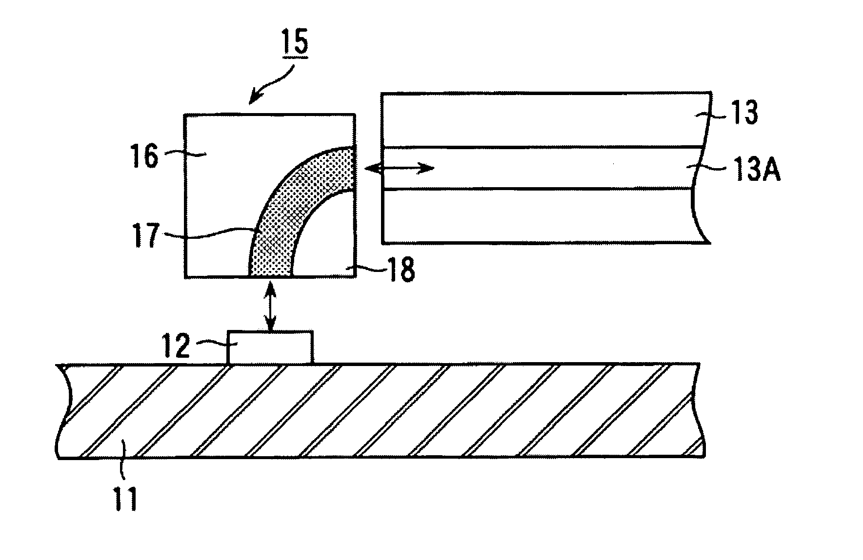
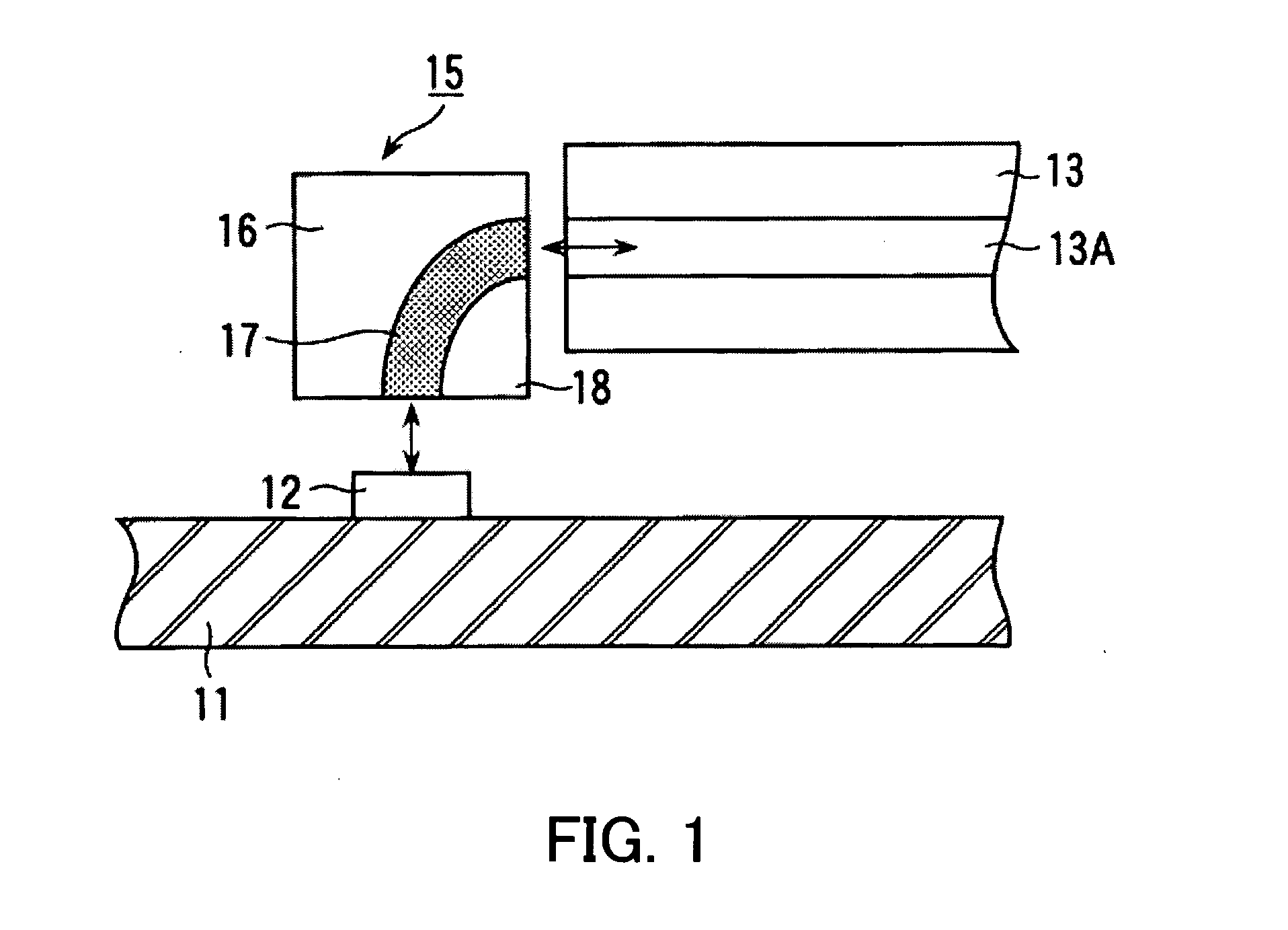
[0095]FIG. 19 is a sectional view of a feature of an optical module for describing an example of the first embodiment of the present invention. In FIG. 19, a printed circuit board 41, a surface type optical device 42, such as a surface emitting laser diode or a photodiode, mounted on the printed circuit board 41, a first clad section 43, a curved surface 43A for turning the course of light gradually and squarely, a lens 43B, a concavity 43C formed in the under surface of the first clad section 43 to cover the surface type optical device 42, a second clad section 45, an optical fiber ribbon 46, and a mechanically transferable (MT) optical connector 47 are shown. A plurality of grooves (not shown) are formed in the direction in which light travels in the curved surface 43A and core sections are formed in these grooves.

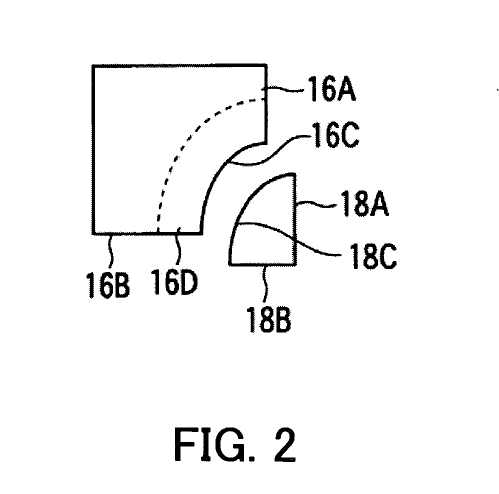
[0096]FIG. 20 is an enlarged sectional view of a portion enclosed by a dashed line in FIG. 19. The same symbols that are used in FIG. 19 indicate the same components or...

second embodiment

[0140]FIGS. 39 through 44 are views for roughly describing processes for fabricating an optical waveguide structure into which lenses are integrated. FIG. 39 is a front view of a feature for roughly describing a first process performed for fabricating an optical waveguide structure into which lenses are integrated. FIG. 40 is a sectional view of the feature for roughly describing the first process performed for fabricating the optical waveguide structure into which the lenses are integrated. FIG. 41 is a front view of a feature for roughly describing a second process performed for fabricating the optical waveguide structure into which the lenses are integrated. FIG. 42 is a sectional view of the feature for roughly describing the second process performed for fabricating the optical waveguide structure into which the lenses are integrated. FIG. 43 is a front view of a feature for roughly describing a third process performed for fabricating the optical waveguide structure into which t...


PUM


Abstract

An optical waveguide structure capable of optically coupling a surface type optical device, such as a surface emitting laser diode or a photodiode, and a transmission medium, such as an optical fiber, located so that their light output surface and light input surface will form an angle of about 90° with each other simply and easily. The optical waveguide structure comprises a first clad section having a curved surface for gradually turning the direction in which light travels almost squarely and a groove formed in the curved surface along the direction in which light travels, a core section which is made from a transparent material with a refractive index higher than the refractive index of the first clad section and with which the groove is filled in, and a second clad section which covers an exposed surface of the core section and the curved surface of the first clad section and which is integrated with the first clad section.

Description

CROSS-REFERENCE TO RELATED APPLICATIONS [0001] This application is based upon and claims the benefits of priority from the prior Japanese Patent Applications No. 2003-325208, filed on Sep. 17, 2003, and No. 2004-252750, filed on Aug. 31, 2004, the entire contents of which are incorporated herein by reference. BACKGROUND OF THE INVENTION [0002] (1) Field of the Invention [0003] This invention relates to an optical waveguide structure suitable for coupling an optical device, such as a laser diode or a photodiode, included in an optical module used for optical communication or optical information processing and a transmission medium, such as an optical fiber or an optical waveguide and an optical module using such an optical waveguide structure. [0004] (2) Description of the Related Art [0005] For example, it is possible to make the integration level of surface emitting laser diodes which form an array higher than that of ordinary edge emitting laser diodes which form an array. That is...

Claims


Application Information

Patent Timeline
Patent Type & Authority Applications(United States)
IPC IPC(8): G02B6/122G02B6/42
CPCG02B6/4204G02B6/4292G02B6/4214G02B6/421
Inventor NISHIZAWA, MOTOYUKITSUKAMOTO, KOJIKATO, MASAYUKIYAMAGISHI, YASUO
Owner FUJITSU LTD
Why Eureka
Try Eureka