System and method for optimized test and configuration throughput of electronic circuits

a technology of electronic circuits and configurations, applied in the field can solve the problems of increased test and configuration costs, increased size and complexity of programmable devices, and significant increase in the cost of testing and configuration of electronic circuits and systems, and achieve the effect of maximizing the throughput of test and configuration and maximizing the maximum achievable throughpu

Inactive Publication Date: 2005-03-17
INTELLITECH INC
View PDF12 Cites 12 Cited by
  • Summary
  • Abstract
  • Description
  • Claims
  • Application Information

AI Technical Summary

Benefits of technology

In accordance with the present invention, a system and method are provided for maximizing the throughput of test and configuration in the manufacture of electronic circuits and systems. The presently disclosed system and method employ a tester having a flexible parallel test architecture with expandable resources that can accommodate a selected number of units under test (UUTs). The parallel test architecture is configurable to accept separate banks or partitions of UUTs, thereby enabling the system to obtain an optimal or maximum achievable throughput of test and configuration for the UUTs. The presently disclosed system and method determine an optimal or maximum achievable throughput by calculating a desired number N of UUTs to be tested / configured in parallel. Testing or configuring this desired number of UUTs in parallel allows the handling time to be balanced with the test and configuration times, thereby resulting in the maximum achievable throughput.
In one embodiment, the system comprises a single test cell and a handling resource for testing and / or configuring a first plurality of N UUTs on a first tester partition, while handling a second plurality of N UUTs on a second tester partition. The single test cell includes a single tester having a parallel test architecture. Because the single tester incurs a minimum amount of idle time, the presently disclosed system achieves maximum utilization of the tester.

Problems solved by technology

In recent years, there has been a significant increase in the cost of testing and configuring electronic circuits and systems.
One factor contributing to the higher test and configuration costs is the increased use of programmable memories such as FLASH, and programmable logic devices such as Complex Programmable Logic Devices (CPLDs) and Field Programmable Gate Arrays (FPGAs).
Another contributing factor is the increased size and complexity of these programmable devices.
As a result, the time required to program such configuration data has increased, thereby increasing manufacturing and end-product costs, which are typically passed along to the customer.
Still another factor contributing to higher product costs is the continuing increase in manufacturing test times. Electronic products are normally tested following fabrication and assembly to assure that no defects have been introduced into the manufacturing process.
As such electronic products have continued to offer more features, higher performance, and reduced size, the ICs and PCBs used to make these products have become more complex and more highly integrated.
This has resulted in increased amounts of test data and increased manufacturing test times, which have further increased manufacturing and end-product costs.
In this way, multiple UUTs can be tested and configured in the same amount of time as a single unit, thereby reducing the effective per-unit test / configuration times. Such techniques can improve throughput, especially when the index times are significantly shorter than the per-unit test and configuration times. However, merely increasing the number of UUTs that are tested and configured in parallel is not always enough to achieve a desired level of throughput, even when massively parallel testing techniques are employed.
Further, parallel testing alone does not always result in the maximum achievable level of throughput.
Moreover, conventional parallel testing techniques are often prohibitive in terms of cost.
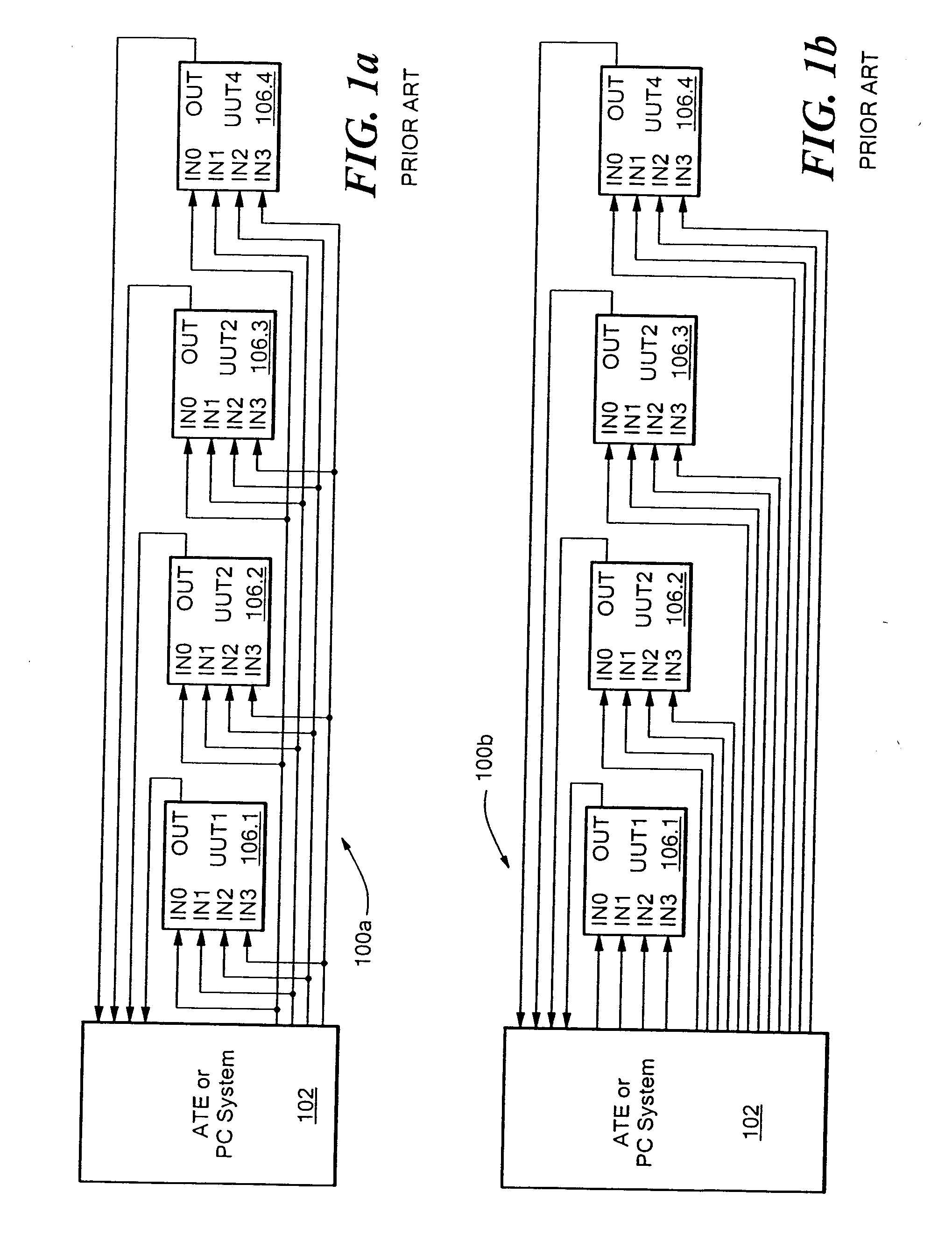
Although conventional testers can be used for ganged and multi-site test and configuration, such testers are typically limited in the number of units that can be tested and configured in parallel.
Such limitations are inherent in the tester's architecture, which depends on individual tester channels and the pattern memory associated with these channels to provide the parallelism required for multi-site testing.
Because the channels and memory are limited in number and capacity in these tester architectures, there is a limit to the number of units that can be tested or configured simultaneously.
As such, conventional tester architectures are not readily scalable for parallel testing, and so their costs often rise prohibitively as the requirements for parallelism and tester resources increase.
However, there is a drawback in that an individual UUT cannot receive test data separate from the other UUTs 106.1-106.4.
However, because PCBs and ICs may have hundreds or even thousands of inputs and outputs, the number of inputs / outputs may rapidly exceed the number of tester channels available, even for relatively small numbers of UUTs.
As such, the ganged test and multi-site test configurations 100a-100b of FIGS. 1a-1b are not readily expandable, and so it is typical that only a relatively small, limited number of UUTs can be tested and configured in parallel with these tester configurations.
However, this can be a costly approach to expanding the tester, and there is still a limit to the number of parallel sites that can be configured for a particular type of UUT.
Although there are alternative ways that ganged and multi-site testing can be configured and performed, these alternative approaches also have limitations in the number of UUTs that can be tested and configured simultaneously.
Such limitations are typically inherent in the ATE architectures and the approaches used.
Further, the number of UUTs that can be tested simultaneously using conventional ATE is often relatively small in number.
Consequently, with these conventional approaches, the number of UUTs that can be handled, tested, and configured in parallel is generally dictated by the limitations of the ATE or PC system, and not the requirements for test and configuration throughput.
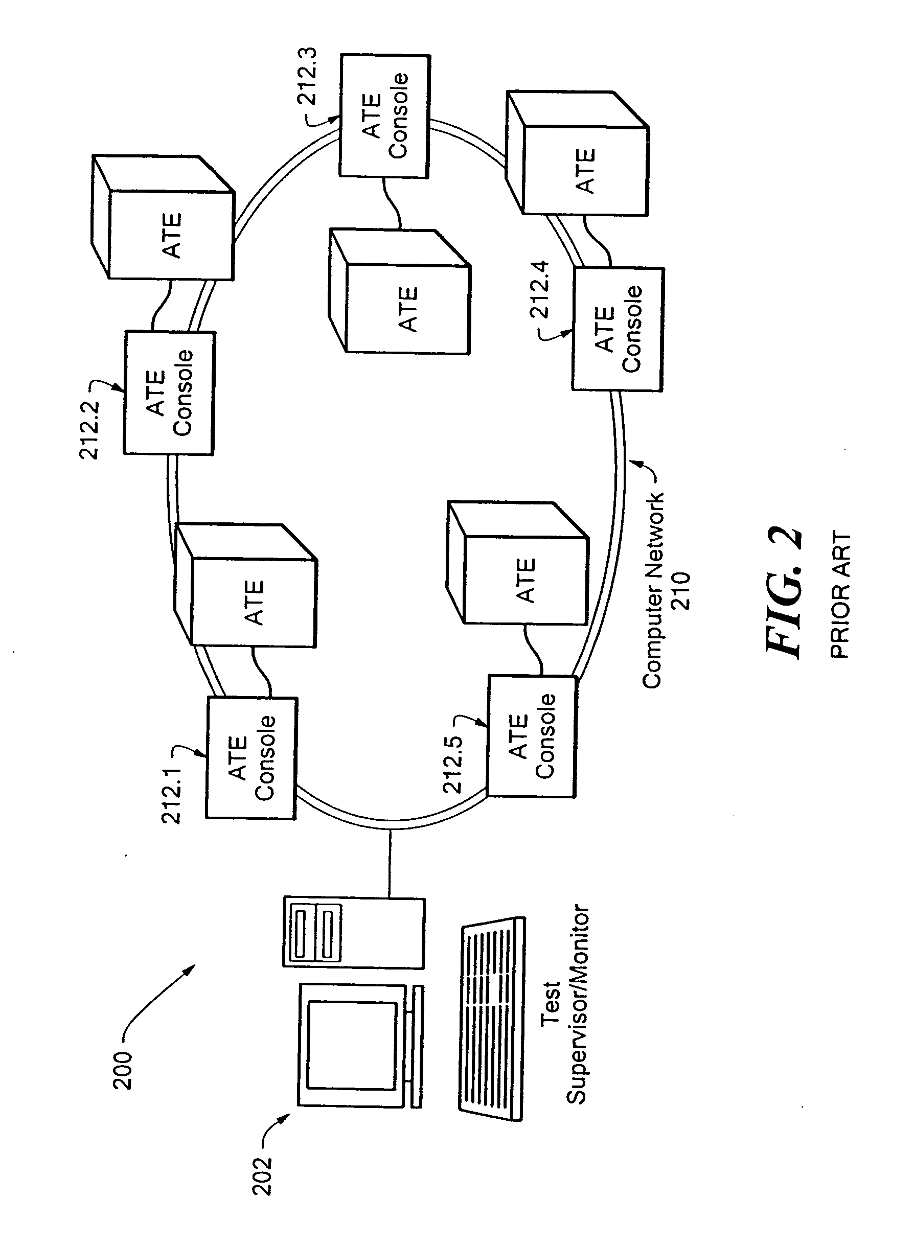
However, expansion using the approach of FIG. 2 can be costly because it typically requires the addition of one or more ATEs and ATE consoles.
However, this approach does not use parallel testing, and typically does not provide for an optimal level of throughput.
Dual well testing only affects the overall throughput by reducing the handling time for removing a tested PCB and inserting another PCB.
Such an arrangement may contribute to signal integrity problems in the test environment, especially when testing high-speed signals on the PCBs.
Accordingly, the conventional techniques described above for providing test and / or configuration of ICs, PCBs, and electronic sub-assemblies and systems are generally incapable of providing an optimal or maximum achievable level of throughput.
Although this is due at least in part to the limitations of the ATE or PC system, it is primarily due to the misconception that simply increasing the number of UUTs tested and configured in parallel will result in an increased throughput.
With a single tester resource, there is little flexibility in adjusting the handling or determining the number of UUTs that can be tested and configured in parallel.
This is because the throughputs are typically dictated by cost and resource limitations of the ATE, e.g., the number of available tester channels compared to the number of pins per die required for configuration and test.
However, this approach can be prohibitive given the costs of adding such expensive capital equipment to a manufacturing line.

Method used


Image

  • System and method for optimized test and configuration throughput of electronic circuits
  • System and method for optimized test and configuration throughput of electronic circuits
  • System and method for optimized test and configuration throughput of electronic circuits

Examples


Embodiment Construction

U.S. Provisional Patent Application No. 60 / 489,312 filed Jul. 23, 2003 entitled SYSTEM AND METHOD FOR OPTIMIZED TEST AND CONFIGURATION THROUGHPUT OF ELECTRONIC CIRCUITS is incorporated herein by reference.

A system and method are disclosed for maximizing the throughput of test and configuration in the manufacture of electronic circuits and systems. The presently disclosed system comprises a single test cell including a single tester having a parallel test architecture, and a handling resource for concurrently testing and / or configuring a plurality of ICs, PCBs, electronic sub-assemblies or systems (units under test, UUTs). An illustrative embodiment of the parallel test architecture employed in the presently disclosed system is described below, followed by a description of a method of balancing the handling time with the test and configuration times to obtain a maximum achievable manufacturing throughput.

Parallel Test Architecture

FIG. 3 depicts an illustrative embodiment of a par...


PUM


Abstract

A system and method for maximizing the throughput of test and configuration in the manufacture of electronic circuits and systems. The system employs a tester having a flexible parallel test architecture with expandable resources that can accommodate a selected number of units under test (UUTs). The parallel test architecture is configurable to accept separate banks or partitions of UUTs, thereby enabling the system to obtain an optimal or maximum achievable throughput of test and configuration for the UUTs. The system determines an optimal or maximum achievable throughput by calculating a desired number N of UUTs to be tested / configured in parallel. Testing or configuring this desired number of UUTs in parallel allows the handling time to be balanced with the test and configuration times, thereby resulting in the maximum achievable throughput.

Description

STATEMENT REGARDING FEDERALLY SPONSORED RESEARCH OR DEVELOPMENT N / A BACKGROUND OF THE INVENTION The present application relates generally to the manufacturing of electronic circuits and systems, and more specifically to a system and method of achieving improved test and configuration throughput of electronic circuits (e.g., integrated circuits (ICs)), printed circuit boards (PCBs), and electronic sub-assemblies and systems. The presently disclosed system and method employ a tester resource (e.g., a computer and controller) that uses a parallel test architecture. Further, the disclosed system and method are operative to calculate an optimal number of units (e.g., ICs or PCBs) to test and / or configure in parallel, thereby allowing manufacturers to achieve both maximum test and configuration throughput and maximum utilization of the tester resource. In recent years, there has been a significant increase in the cost of testing and configuring electronic circuits and systems. One fact...

Claims


Application Information

Patent Timeline
Patent Type & Authority Applications(United States)
IPC IPC(8): G01R31/00G01R31/28G01R31/3185G01R31/319G06F17/00H05K
CPCG01R31/31926G01R31/318533
Inventor CLARK, CHRISTOPHER J.RICCHETTI, MICHAEL
Owner INTELLITECH INC
Why Eureka
Try Eureka