Fabrication of nanoscale thermoelectric devices

a thermoelectric device and nano-scale technology, applied in the direction of thermoelectric device manufacturing/treatment, printed circuit manufacturing, conductive pattern formation, etc., can solve problems such as damage to nanowires

Inactive Publication Date: 2005-03-24
CANON KK
View PDF14 Cites 47 Cited by
  • Summary
  • Abstract
  • Description
  • Claims
  • Application Information

AI Technical Summary

Problems solved by technology

As noted above, nanostructures tend to be fragile and any physical impact, by methods such as grinding or shaving, may cause damage to the nanowires.

Method used


Image

  • Fabrication of nanoscale thermoelectric devices
  • Fabrication of nanoscale thermoelectric devices
  • Fabrication of nanoscale thermoelectric devices

Examples


Embodiment Construction

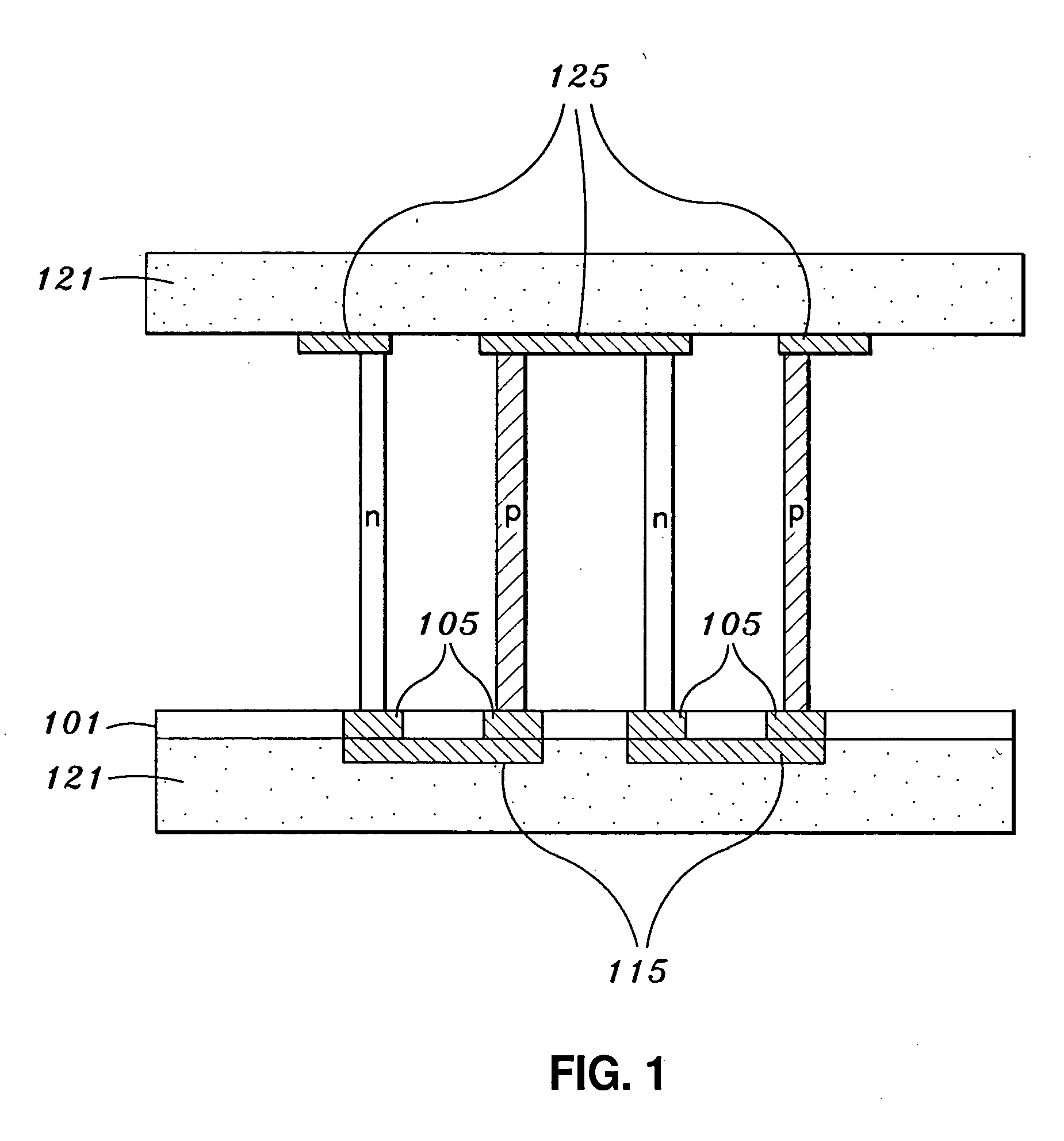
The present invention provides a method for fabricating a nanoscale thermoelectric module, wherein the thermoelements are nanowire structures. The TEM produced is expected to have more efficient thermoelectric qualities due to the nanowire thermoelements. Furthermore, the fabrication method that is provided is likely to yield numerous advantages, such as a decreased likelihood of damage to the nanowires during device fabrication, adaptability to automation and lower manufacturing costs.

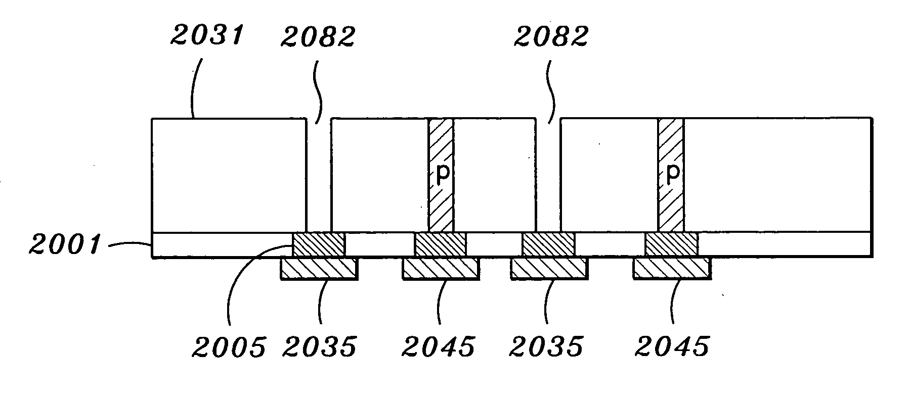
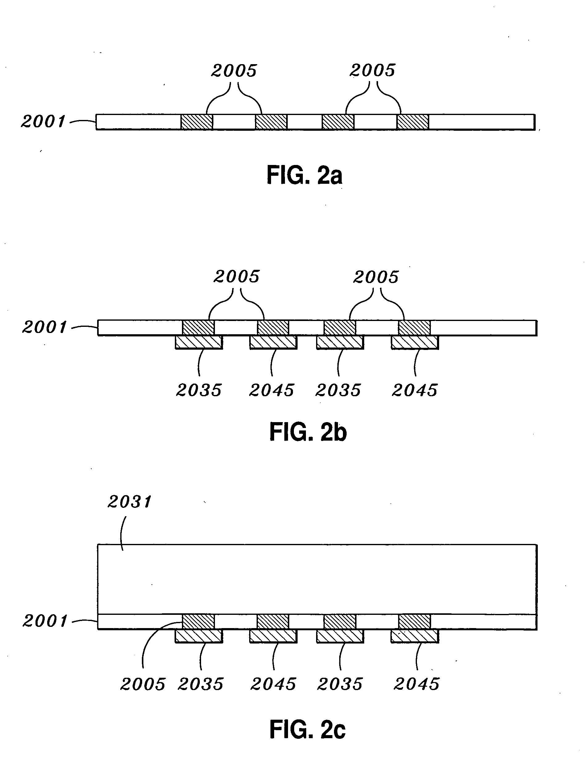
FIGS. 2a through 2g show various stages of one embodiment of the method of the present invention from a cross-sectional view. FIGS. 4a to 4c show a bottom view of select stages of TEM fabrication.

One feature of the present invention is the use of a substrate with through-electrodes upon which the p-type and n-type nanowires are to be grown, an example of which is shown in FIG. 2a. FIG. 4a shows the bottom view of the substrate shown in FIG. 2a. The substrate (2001) has substrate electrodes (2005) ...


PUM

PropertyMeasurementUnit
diameteraaaaaaaaaa
diameteraaaaaaaaaa
diameteraaaaaaaaaa

Abstract

The present invention concerns a method for fabricating a nanowire thermoelectric device comprising the step of providing a substrate upon which to form nanowires. The substrate comprises substrate electrodes passing from a top exposed surface of the substrate to a bottom exposed surface of the substrate. Another step involves forming a first electrode pattern, which forms first and second electrically connected groups of substrate electrodes, on the bottom surface of the substrate. A p-type nanowire is then formed on the substrate by activating the first group of substrate electrodes during p-type material deposition. Similarly, a n-type nanowire is formed by activating the second group of substrate electrodes during n-type material deposition. And top electrodes are formed to connect the p-type and the n-type nanowires and a second electrode pattern is formed on the bottom side of the substrate to replace the first electrode pattern to form a thermocouple.

Description

BACKGROUND AND SUMMARY 1. Field of the Invention The present invention generally relates to a method for fabricating nanowire thermoelectric devices. 2. Description of the Related Art Nanowires are known in the art as wire structures which have a diameter measured in hundreds of nanometers (nm) or less, typically measured from 1 to 500 nm. When devices are constructed using structures of such a small scale, quantum mechanical rules and phenomena begin to have a greater effect on the operation of such devices in comparison to larger scale structures. The increased role and effect of quantum mechanics is due to the reduced number of atoms and electrons present in the system, which makes their discrete quantum natures more apparent. While it is not known how quantum mechanics will affect the operation of all nanoscale devices, it has been found that thermoelectric modules (TEMs) constructed using nanowires are likely to show increased efficiency relative to even microsized TEM dev...

Claims


Application Information

Patent Timeline
Patent Type & Authority Applications(United States)
IPC IPC(8): H01L35/32H01L35/34H05K3/02H05K3/20
CPCH01L35/32H01L35/34Y10T29/49128Y10T29/49155Y10T29/49194H10N10/01H10N10/17
Inventor OKAMURA, YOSHIMASAKOHLER, TIMOTHY L.MIYAWAKI, MAMORU
Owner CANON KK
Why Eureka
Try Eureka