Sensor device having thin membrane and method of manufacturing the same
a technology of a sensor device and a thin membrane, which is applied in the direction of acceleration measurement using interia forces, instruments, liquid/fluent solid measurement, etc., can solve the problems of common damage to the thin membrane formed by the insulating film, and achieve the effect of preventing damag
- Summary
- Abstract
- Description
- Claims
- Application Information
AI Technical Summary
Benefits of technology
Problems solved by technology
Method used
Image

Examples
first embodiment
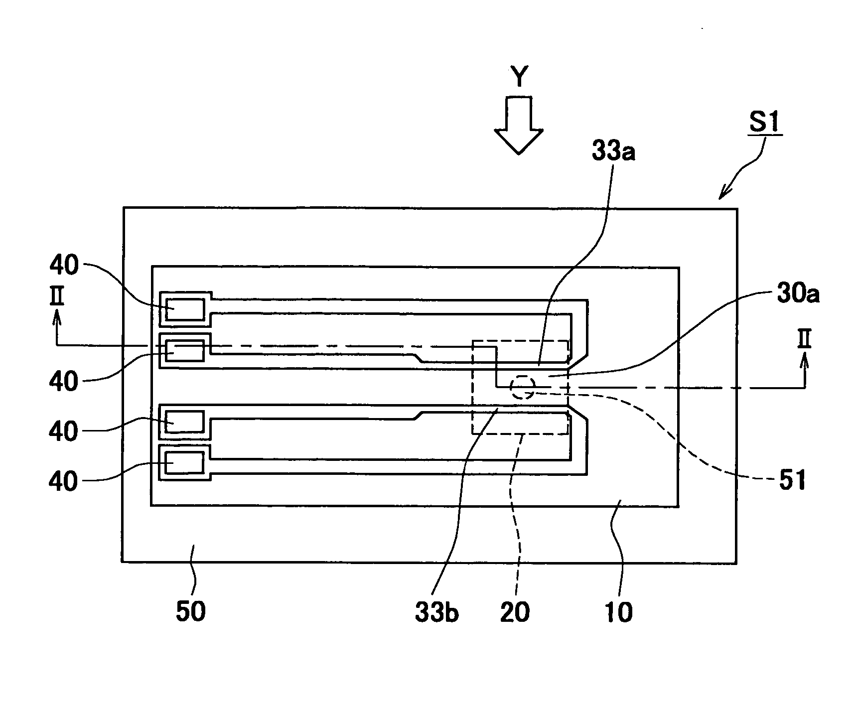
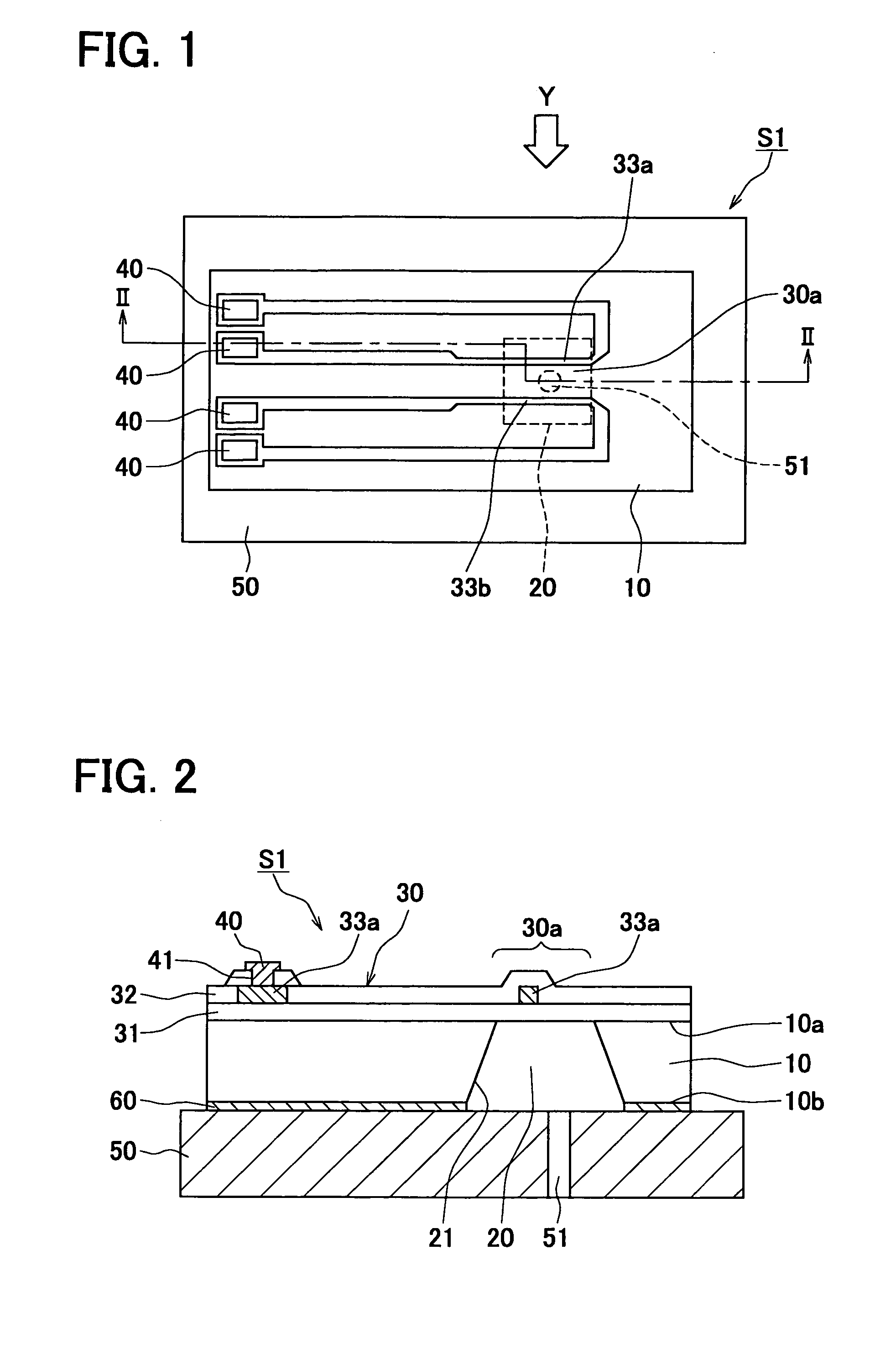
[0020] the present invention will be described with reference to FIGS. 1-3. FIGS. 1 and 2 show an airflow sensor S1 to which the present invention is applied. As better seen in FIG. 2, the airflow sensor S1 is composed of a silicon substrate 10 having a first surface 10a and a second surface 10b, laminated layers 30 formed on the first surface 10a and a base plate 50 bonded to the second surface 10b with an adhesive 60. A cavity 20 is formed in the silicon substrate 10 by anisotropic etching or the like. The cavity 20 has an opening 21 open to the second surface 10b of the silicon substrate 10, and its first surface side is closed with the laminated layers 30.
[0021] The laminated layers 30 include a first insulation layer 31 and a second insulation layer 32 laminated in this order on the first surface 10a of the silicon substrate 10. The laminated layers 30 also include thin film resistors 33a and 33b positioned on the cavity 20. Both insulation layers 31, 32 are formed to cover an ...
second embodiment
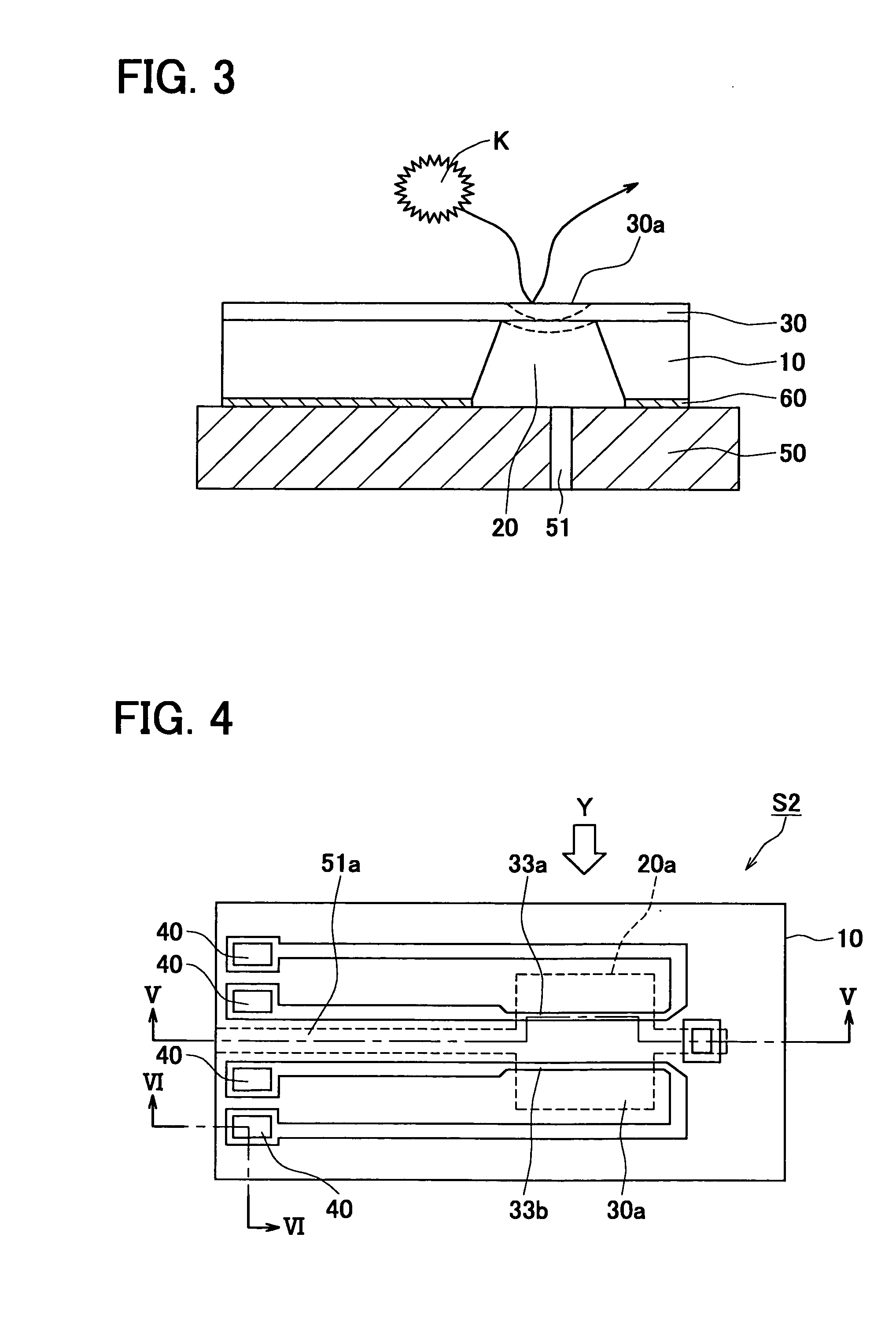
[0044] The airflow sensor S2 having the cavity 20a and the thin membrane 30a can be easily manufactured in the process described above. That is, the cavity 20a and the air passage 51a are simultaneously formed by removing the sacrificial layer 110 by etching. Further, the air passage 51a is exposed to the side surface of the silicon substrate at the same time when the wafer having plural sensor chips is diced into individual sensor chips. Though the thin membrane 30a facing the cavity 20a is formed on the first surface 10a of the silicon substrate 10 in the second embodiment, it is also possible to additionally form the same structure on the second surface 10b.
[0045] A third embodiment of the present invention will be described with reference to FIGS. 8 and 9. In FIG. 9, an airflow sensor S3 is shown as a third embodiment of the present invention, and in FIG. 8, a process of manufacturing the airflow sensor S3 is shown. As shown in FIG. 9, the airflow sensor S3 includes a first sil...
third embodiment
[0048] The airflow sensor S3 includes the cavity 20b formed in the first silicon layer 310 and the thin air passage 51b connecting the cavity 20b to the outside air. The size of the air passage 51b is made much smaller than the cavity 20b as done in the foregoing embodiments. When air flows through the air passage 51b, a predetermined pressure loss occurs therein. The advantages obtained in this third embodiment are the same as those in the foregoing embodiments. That is, the pressure in the cavity 20b is kept constant if the temperature changes, and a rapid pressure change in the cavity 20b caused by collision of foreign particles with the thin membrane 30a is alleviated by damper effect of the cavity 20b.
[0049] The present invention is not limited to the embodiments described above, but it may be variously modified. For example, this invention is applicable to various sensors having a thin membrane, on which a sensing element is formed, other than the airflow sensor. The sensors ...
PUM
 Abstract
Description
Claims
Application Information
 - R&D Engineer
- R&D Manager
- IP Professional
- Industry Leading Data Capabilities
- Powerful AI technology
- Patent DNA Extraction
Browse by: Latest US Patents, China's latest patents, Technical Efficacy Thesaurus, Application Domain, Technology Topic.
© 2024 PatSnap. All rights reserved.Legal|Privacy policy|Modern Slavery Act Transparency Statement|Sitemap