
Eureka
For R&D, Eureka makes reading and utilizing patents & technical documents easy.
Eureka AIR
Designed for self-driven R&D workflows. Generate viable solutions, solve complex R&D challenges, empower your innovation with AI.

Eureka Materials
Designed for material experts only. Revolutionize your material R&D, from search, analyze, to developing new materials.

TechResearch
Generate reliable direction feasibility study reports for your R&D in just a few steps.

TechSeek
Discover and master advanced knowledge NOW. Basics, ideas, possibilities, all at once.

TechMind
As an expert in R&D Theories, TechMind can generates customized viable solutions instantly.

TechRisk
Analyze your overall solution with one click, know your potential R&D risks in advance.

TechMonitor
Get weekly tech updates, stay abreast of the latest tech innovations and key insights.
Device for electrical connection between two wafers and fabrication process of a microelectronic component comprising such a device
- Summary
- Abstract
- Description
- Claims
- Application Information
AI Technical Summary
Benefits of technology
Problems solved by technology
Method used
Image

Examples
Embodiment Construction
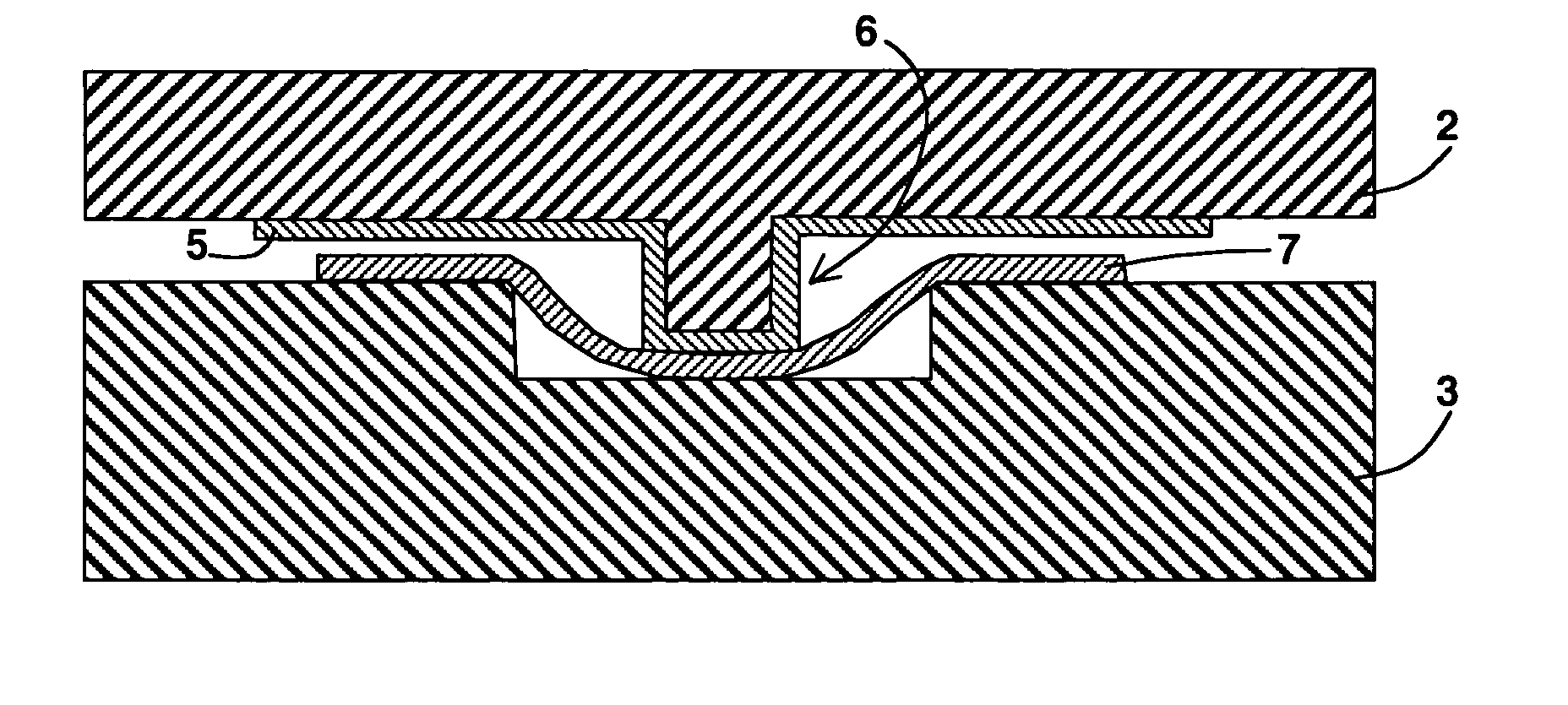
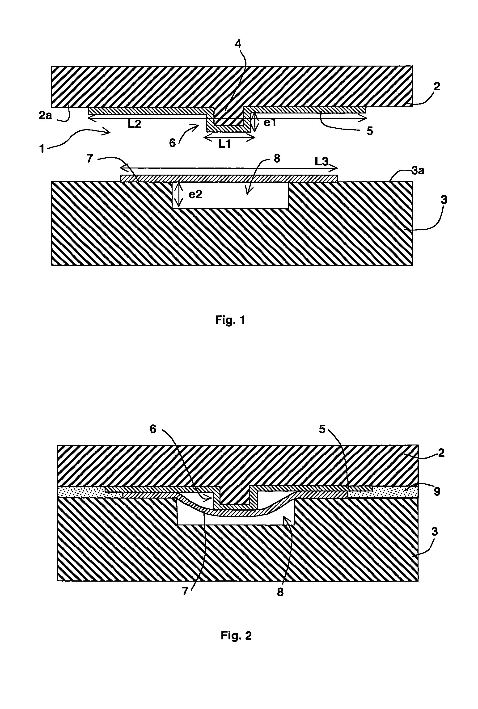
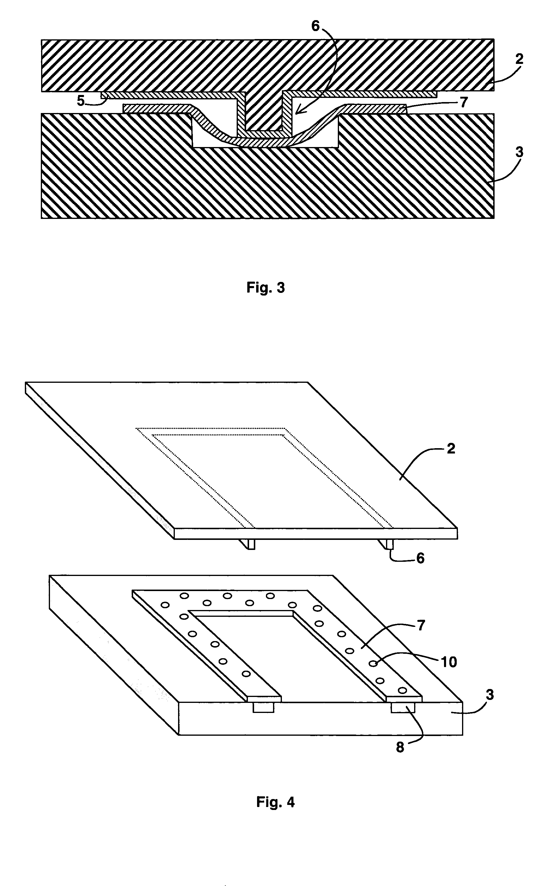
[0021] As represented in FIG. 1, in a microelectronic component comprising first and second wafers 2 and 3, an electrical connection device 1 comprises at least first and second contact elements respectively integral to the opposite faces 2a et 3a of the first and second wafers 2 and 3. The first and second contact elements are designed to be placed in contact with one another to achieve an electrical connection when the first and second wafers are assembled. Each wafer 2 or 3 can for example be made of silicon or glass. Thus, the first wafer can for example form a substrate whereon an integrated circuit is arranged whereas the second wafer can be a substrate whereon there is arranged a Micro Electro Mechanical System (MEMS).
[0022] Thus, in FIG. 1, the face 2a of the first wafer 2 comprises a protrusion 4 and a metallic layer 5 is arranged on the face 2a, so as to cover the protrusion 4 and to form a salient zone 6. The metallic layer 5 preferably has a greater width L2 than the wi...
PUM
 Abstract
Description
Claims
Application Information
 - R&D Engineer
- R&D Manager
- IP Professional
- Industry Leading Data Capabilities
- Powerful AI technology
- Patent DNA Extraction
Browse by: Latest US Patents, China's latest patents, Technical Efficacy Thesaurus, Application Domain, Technology Topic, Popular Technical Reports.
© 2024 PatSnap. All rights reserved.Legal|Privacy policy|Modern Slavery Act Transparency Statement|Sitemap|About US| Contact US: help@patsnap.com