Memory module and memory support module

a memory module and memory support technology, applied in the field of memory modules and memory support modules, can solve problems such as unsolved problems, and achieve the effect of reliably switching the memory clock and enabling the supply of signals to memory chips

Inactive Publication Date: 2005-03-31
MELCO INC
View PDF1 Cites 18 Cited by
  • Summary
  • Abstract
  • Description
  • Claims
  • Application Information

AI Technical Summary

Benefits of technology

[0039] When the memory module is connected to the first computer, the computer further supplies the memory circuit with the pulse-shaped clock signal and a plurality of clock enable signals for each of a plurality of memory spaces having capacities corresponding to the second specified number of address signals. At this time, the memory circuit generates the memory clock enable signal based on the plurality of clock enable signals. The memory chip is supplied with the generated memory clock enable signal together with the clock signal. Accordingly, the memory chip becomes operative when the memory clock enable signal is enabled. That is to say, when the computer outputs a plurality of clock enable signals to a plurality of memory spaces, the memory chip can be accessed appropriately.
[0040] As mentioned above, it is possible to reliably switch the memory clock enable signal to be supplied to memory chips.

Problems solved by technology

The problem remains unsolved.

Method used


Image

  • Memory module and memory support module
  • Memory module and memory support module
  • Memory module and memory support module

Examples


modification examples

(3) Modification Examples

[0110] The memory module according to the present invention may be embodied in various modification examples.

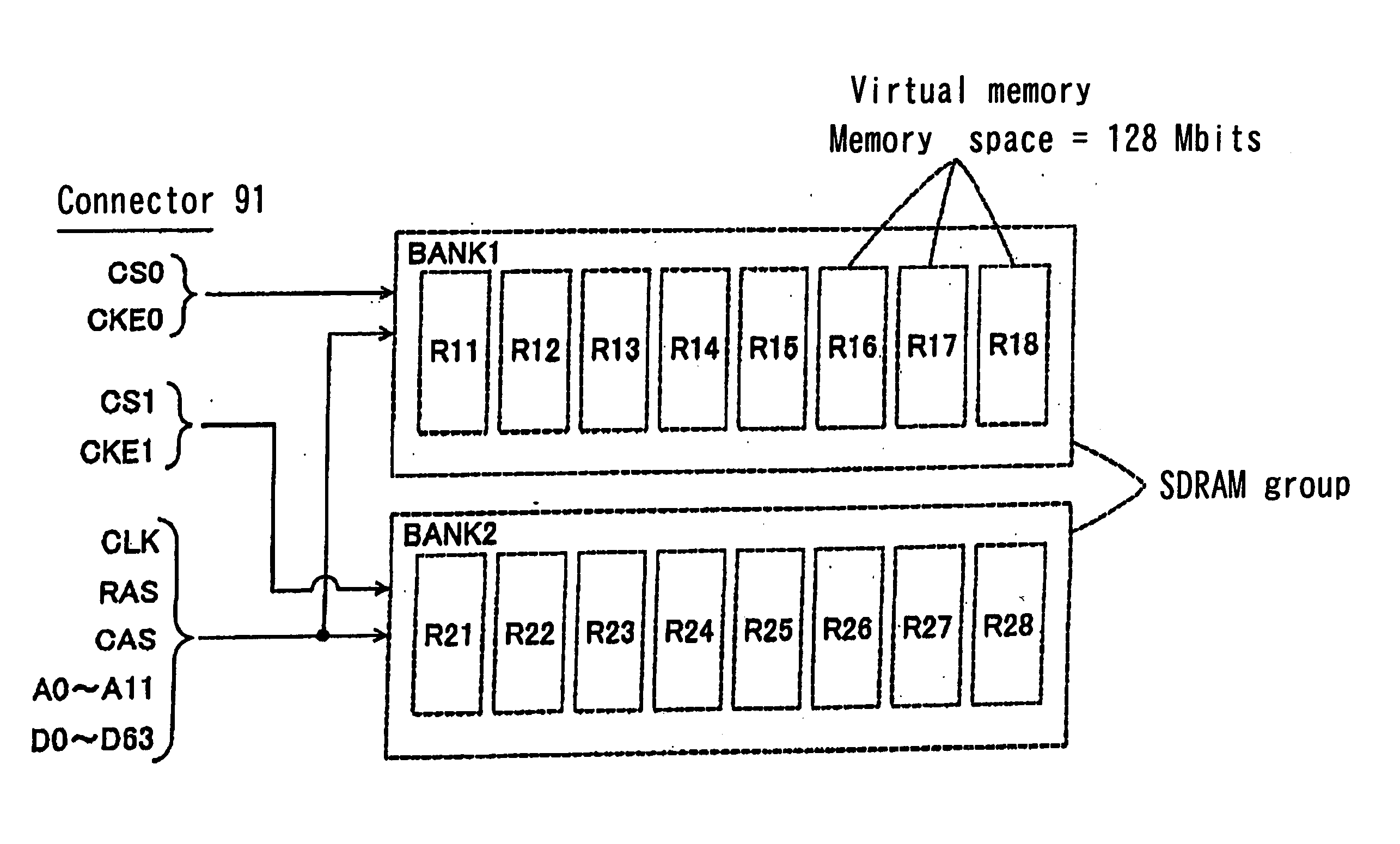
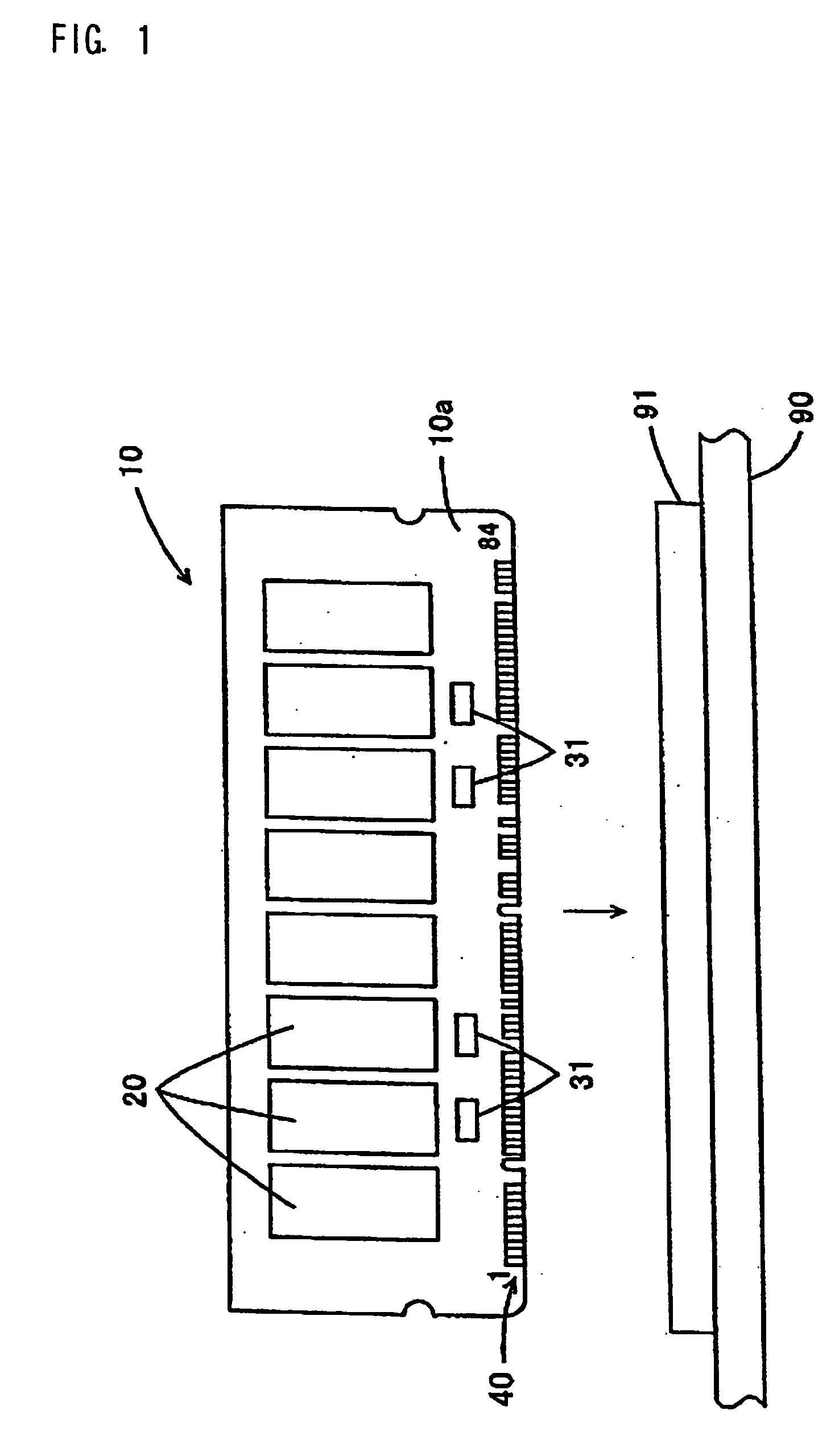
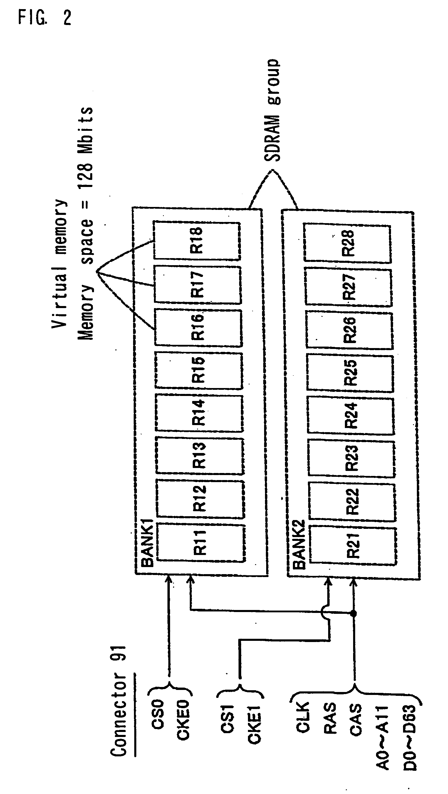
[0111] While the above-mentioned memory module 10 represents DIMMs having no ECC (Error Correction Code), the present invention can be applied to memory modules with ECC simply requiring an addition of ECC memory. Of course, the present invention can be applied to not only DIMMs, but also SIMMs and the like.

[0112] Some SDRAMs use 16 data signal input / output terminals. The present invention can be applied even to such memories to effectively use memory areas. In this case, the memory needs to be able to accept a plurality of address signals more than the second specified number of address signals generated by the computer. Of course, the present invention can be applied to memories that do not use eight or 16 data signal input / output terminals. Further, the present invention can be applied to ROMs and the like that can only read data.

[0113] Moreover...


PUM


Abstract

It is aimed at not only enabling access to an inaccessible SDRAM area from a PC which only outputs A0 through A11 signals, but also making a common memory module connectable to earlier or latest PCs independently of their models. According to the construction, a connected PC (computer) inputs a high-order address signal A12. It is determined whether or not the input A12 signal is set to a state different from an unused state. A determination signal is generated so as to indicate a state corresponding to a determination result. When the determination signal indicates a changed state, the PC inputs A0 through A12 signals and supplies them to a memory chip 20. When the determination signal indicates an unchanged state, the PC inputs A0 through A11 signals and a select signal. The A12 signal is generated based on the input select signal. The memory chip 20 is supplied with the A12 signal and the input A0 through A11 signals.

Description

BACKGROUND OF THE INVENTION [0001] 1. Field of the Invention [0002] The present invention relates to a memory module and a memory support module connectable to a computer body. [0003] 2. Description of Related Art [0004] Conventionally, computer memories are expanded by connecting a memory module to a computer's socket (slot) Available memory modules include a 128-Mbyte DIMM (Dual Inline Memory Module) comprising eight 128-Mbit SDRAM (Synchronous Dynamic Random Access Memory) chips and a 256-Mbyte DIMM comprising 16 128-Mbit SDRAM chips. Normally, the 128-Mbit SDRAM is provided with 12 address signal terminals A0 through A11 connectable to 12 signal lines for row addresses and 10 signal lines for column addresses. When a computer inputs address signals A0 through A11, it is possible to read or write data at the corresponding addresses for all 128-Mbit areas in the entire SDRAM. [0005] The above-mentioned 256-Mbyte DIMM is divided into two blocks (banks) of SDRAM groups. In addition ...

Claims


Application Information

Patent Timeline
Patent Type & Authority Applications(United States)
IPC IPC(8): G06F12/06G06F12/00
CPCG06F12/0669
Inventor BUNGO, MOTOHIKO
Owner MELCO INC
Why Eureka
Try Eureka