

Integration of sensor based metrology into semiconductor processing tools
- Summary
- Abstract
- Description
- Claims
- Application Information
AI Technical Summary
Problems solved by technology
Method used
Image

Examples
Embodiment Construction
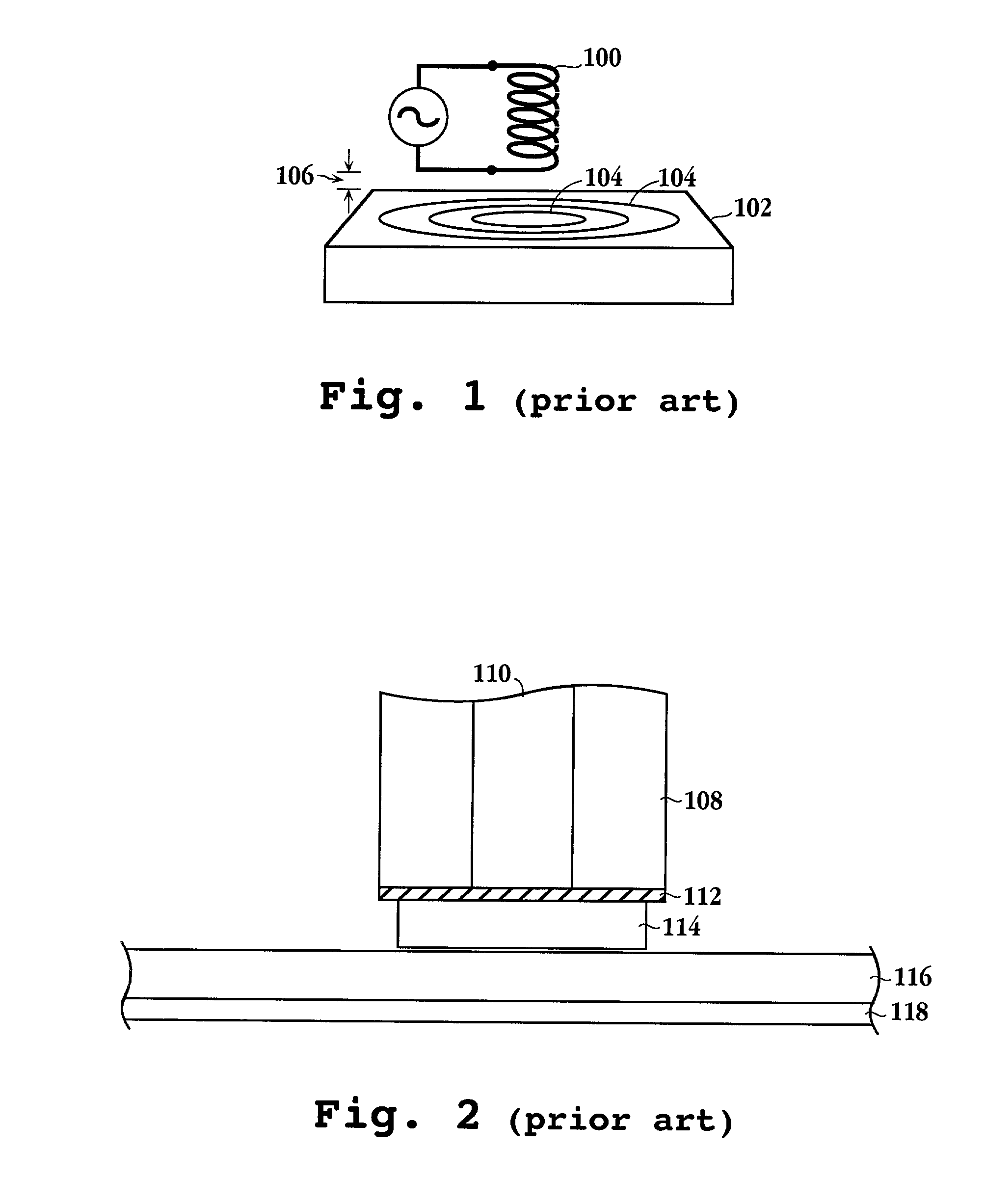
[0037] Several exemplary embodiments of the invention will now be described in detail with reference to the accompanying drawings. FIGS. 1 and 2 are discussed above in the “Background of the Invention” section.
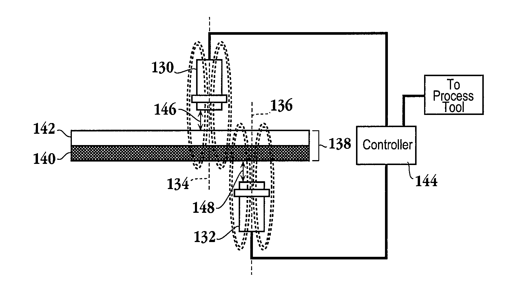
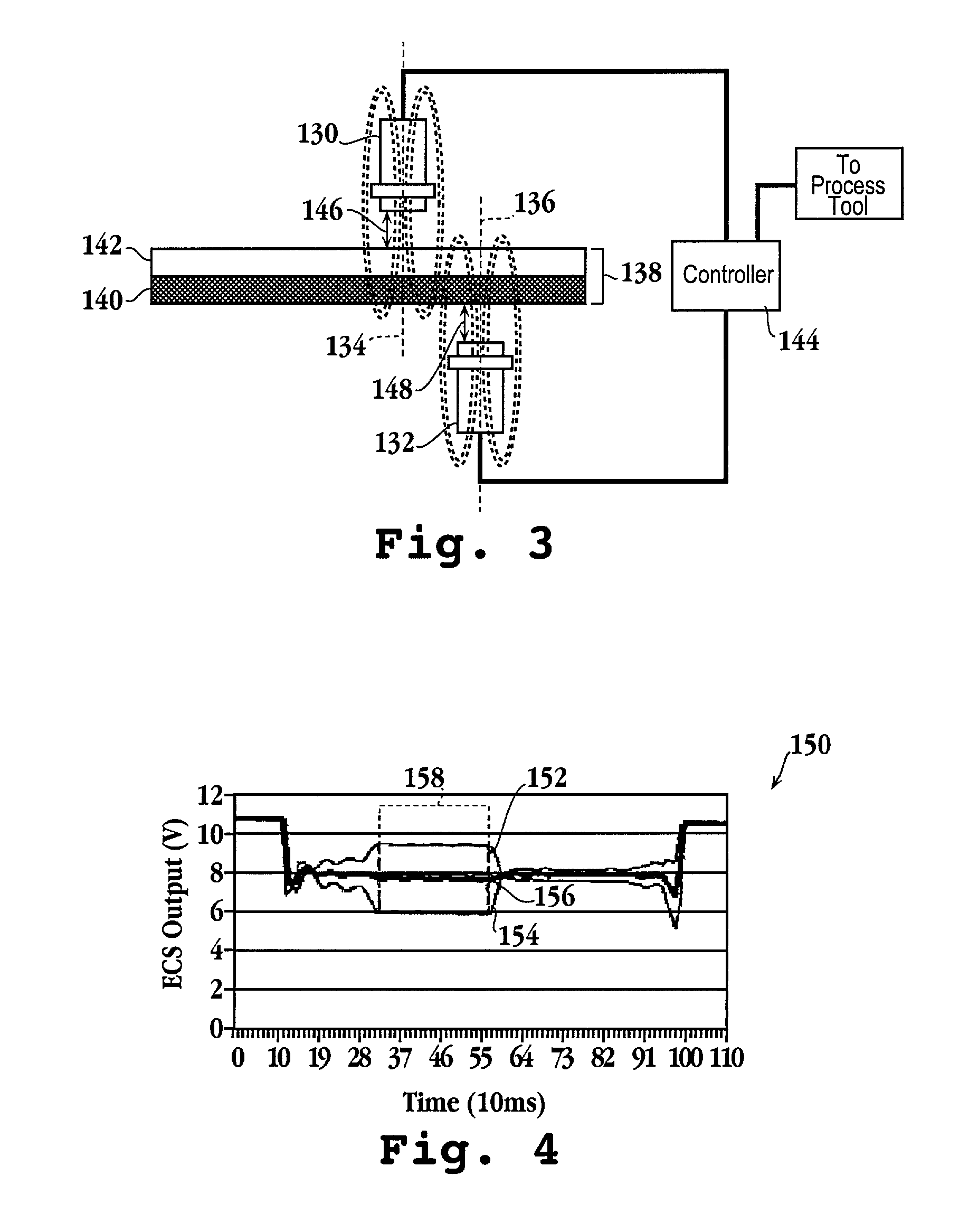
[0038] Eddy current sensors (ECS) allow for measuring a metal film thickness of a moving wafer. It has been determined that ECS are capable of providing a fast enough response for a wafer moving under typical loading robotics velocity. Therefore, it is possible to perform the thickness measurements “on the fly” without impacting process throughput. Moreover, the movement of the wafer can be taken advantage of to produce a thickness profile from a limited number of sensors in a cluster configuration. For example, wafer aligners provide movement in a rotational direction and a linear radial direction. Accordingly, a cluster of sensors can capture a thickness profile of a wafer while the wafer is undergoing common automated wafer handling schemes. In one embodiment, a thickness ...
PUM
| Property | Measurement | Unit |
|---|---|---|
| Thickness | aaaaa | aaaaa |
| Pressure | aaaaa | aaaaa |
| Distance | aaaaa | aaaaa |
Abstract
Description
Claims
Application Information