Semiconductor device with a toroidal-like junction

a semiconductor and toroidal technology, applied in the direction of semiconductor devices, electrical apparatus, transistors, etc., can solve the problems of unimportant limit of resolution and depth of focus, and achieve the effect of great utility and importan

Inactive Publication Date: 2005-04-07
ATMEL CORP
View PDF3 Cites 6 Cited by
  • Summary
  • Abstract
  • Description
  • Claims
  • Application Information

AI Technical Summary

Problems solved by technology

Thus, limit-of-resolution and depth-of-focus are unimportant parameters.

Method used


Image

  • Semiconductor device with a toroidal-like junction
  • Semiconductor device with a toroidal-like junction
  • Semiconductor device with a toroidal-like junction

Examples


Embodiment Construction

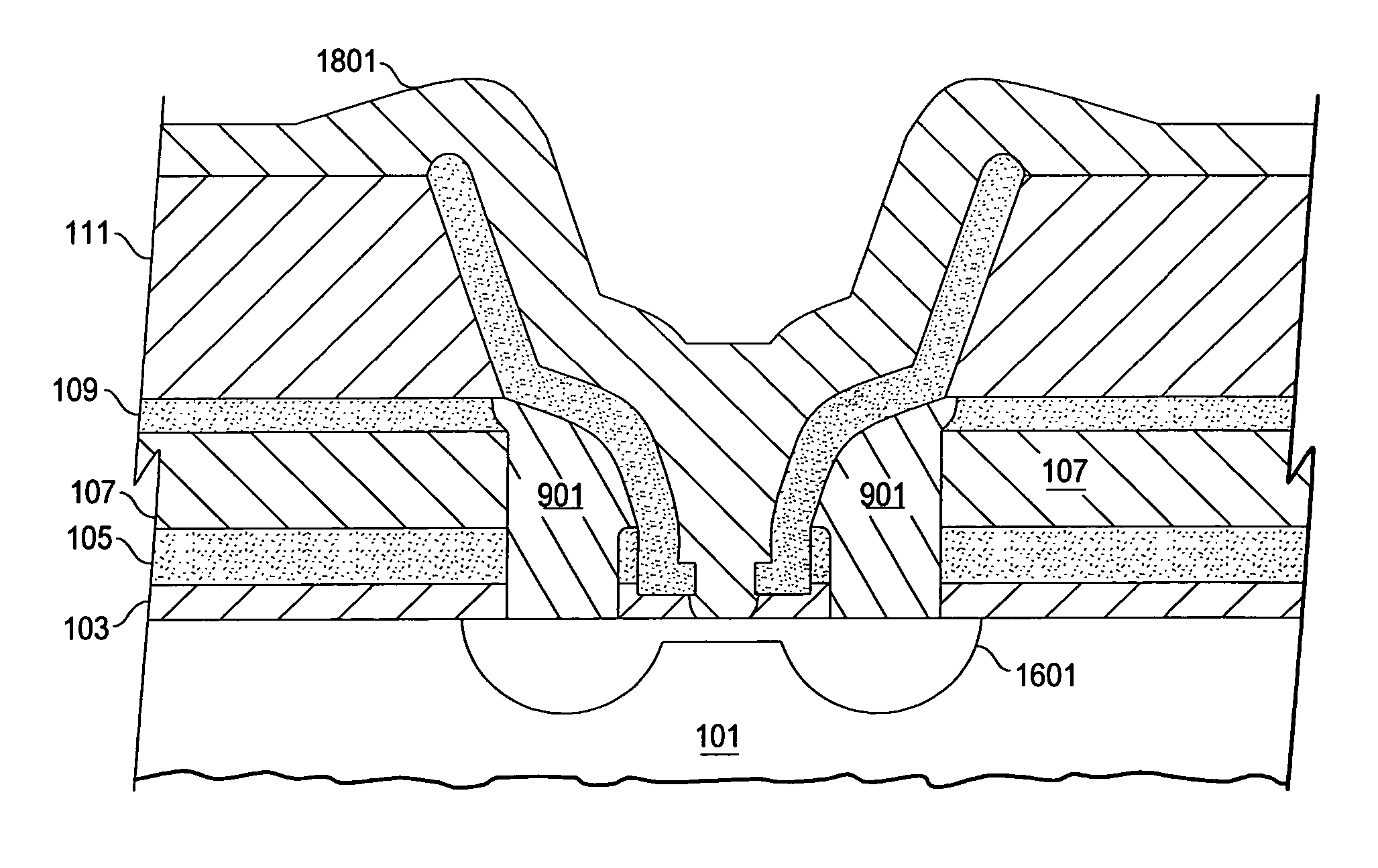
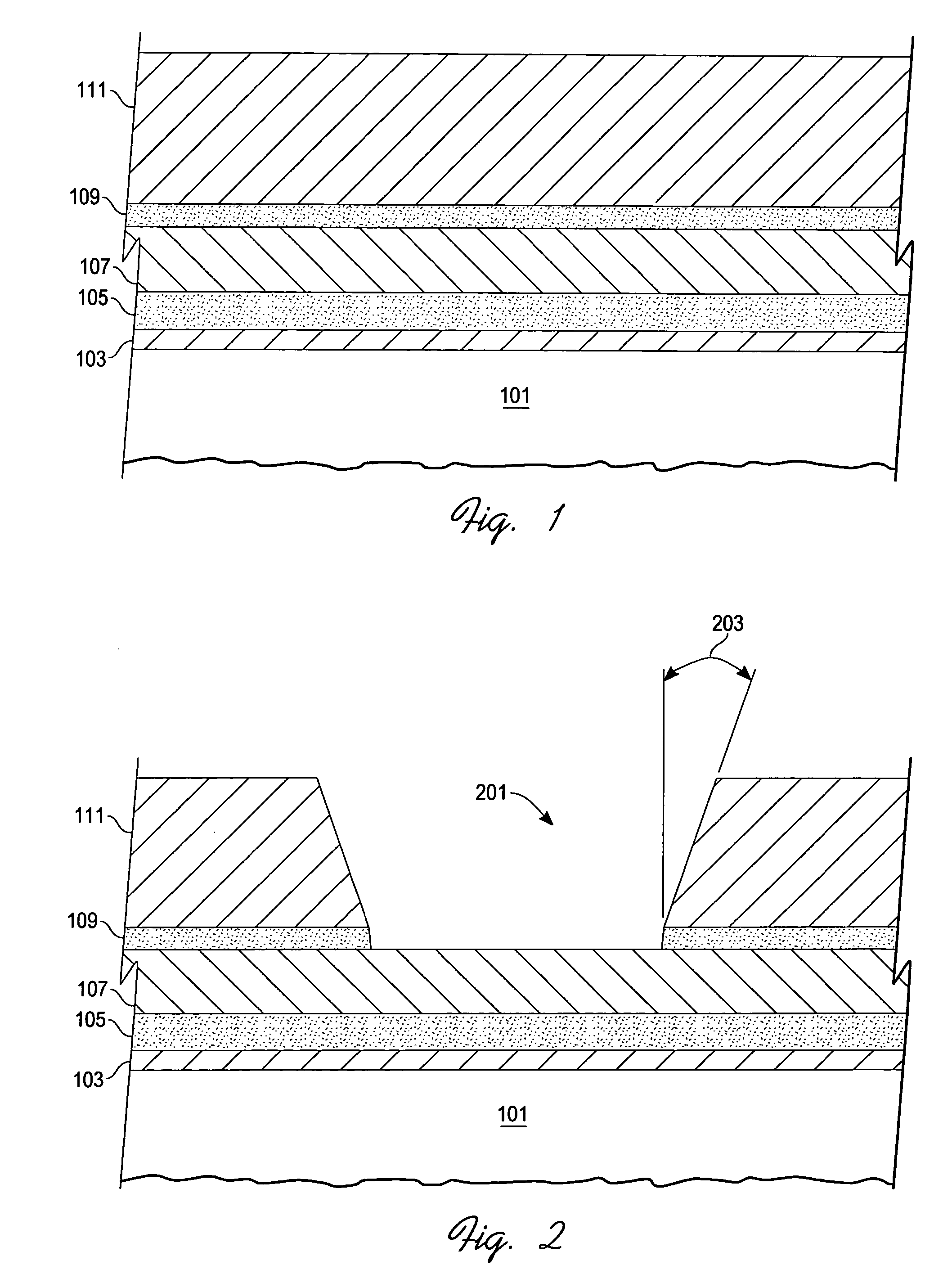
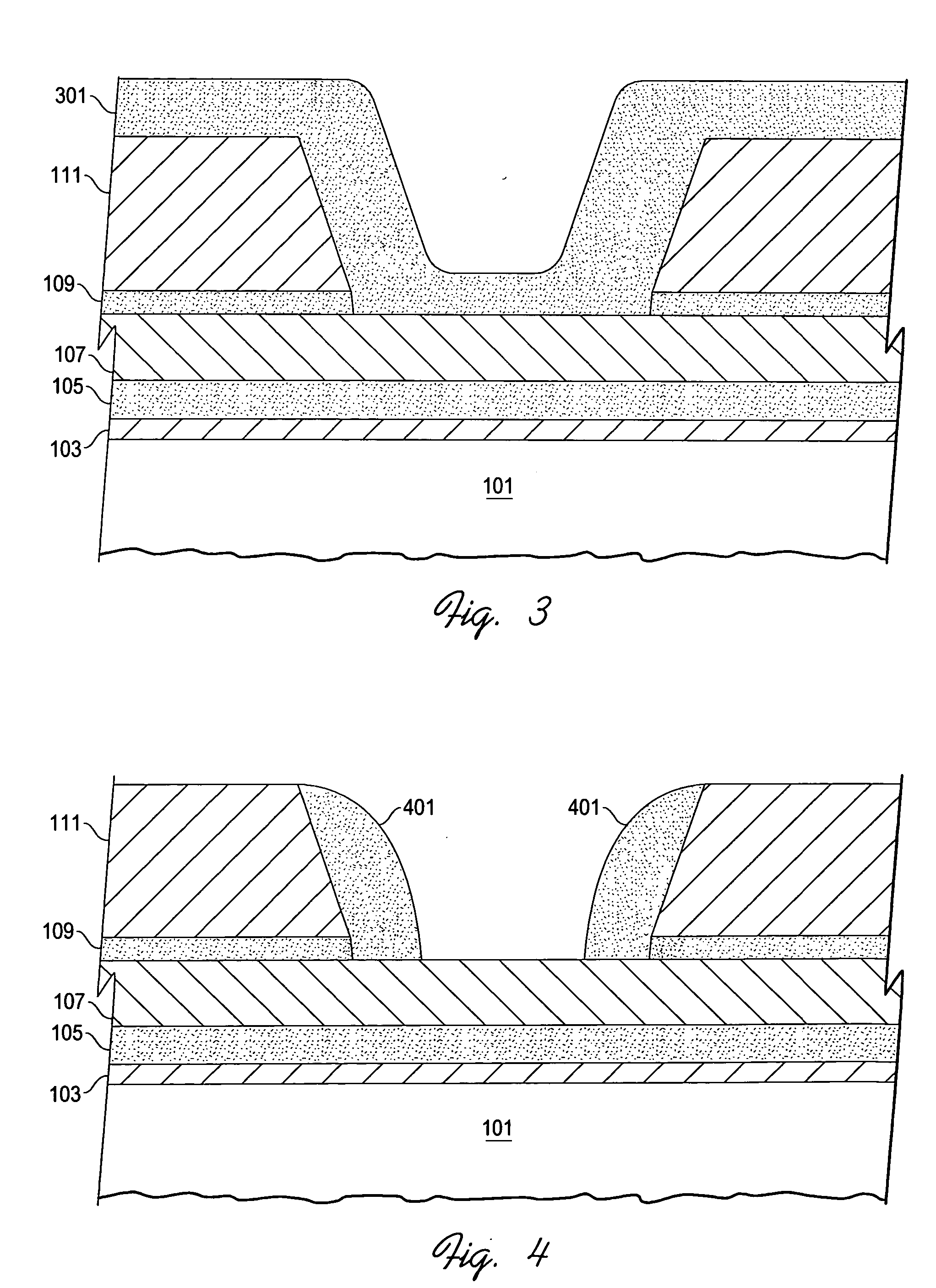
With reference to FIGS. 1-18, an exemplary embodiment of the present invention is described in detail according to the following process steps. To start, FIG. 1 shows an exemplary embodiment of a cross-sectional view of deposited films used to form an electronic device structure. Each film layer is deposited in compliance with process steps that are well-known in the semiconductor art. FIG. 1 includes a base substrate 101, a pad oxide 103, a first nitride layer 105, a first polycrystalline silicon (“poly”) layer 107, a second nitride layer 109, and an isolation oxide 111.

In a specific exemplary embodiment, nominal film thicknesses and methods of deposit are provided as follows; the pad oxide is a thermally grown 400 Å oxide, the first nitride is 1000 Å thick, the first poly is 1800 Å thick, the second nitride layer is 700 Å thick, and the isolation oxide is 7000 Å thick, deposited by a plasma-enhanced chemical vapor deposition (PECVD) process.

The base substrate 101 is frequentl...


PUM


Abstract

Formation of elements of a vertical bipolar transistor is described, in particular a vertical npn transistor formed on a p-type substrate. Accordingly, an improved method not limited by constraints of photolithography, and an ensuing device made by such methods, is described. A temporary spacer (e.g., an oxide spacer) is deposited over a dielectric separation layer. The temporary spacer and dielectric separation layers are then anisotropically etched, forming a dielectric “boot shape” on a lower edge of the dielectric separation layer. An area within this non-photolithographically produced boot region defines an emitter contact window. Since the boot tip is formed through deposition and etching techniques, the emitter window is automatically aligned (i.e., self-aligned) with an underlying base region. Feature sizes are determined by deposition and etching techniques. Consequently, photolithography of small features is eliminated.

Description

TECHNICAL FIELD This invention relates generally to a process for fabricating an integrated circuit structure, and more specifically to electronic devices having semiconductor junctions and to a process for their manufacture. BACKGROUND ART There is a need in the integrated circuit art for obtaining increasingly smaller devices without sacrificing device performance. The small device size requires small device regions, precise and accurate alignment between regions and minimization of parasitic resistances and capacitances. Device size can be reduced by putting more reliance on fine line lithography, but as discussed below, it becomes impractical or impossible to continue to reduce feature size and achieve the required greater increase in alignment accuracy. As lithography is pushed to the limit, yield and production throughput decrease. Four governing performance parameters of a photolithographic system are limit-of-resolution, Lr, level-to-level alignment accuracy, and depth-of...

Claims


Application Information

Patent Timeline
Patent Type & Authority Applications(United States)
IPC IPC(8): H01L21/28H01L21/336H01L21/8238H01L29/423H01L29/786
CPCH01L21/28123H01L21/823885H01L29/78642H01L29/66742H01L29/66772H01L29/42384
Inventor LOJEK, BOHUMIL
Owner ATMEL CORP
Why Eureka
Try Eureka