Method and apparatus for driving plasma display panel

Inactive Publication Date: 2005-04-14
LG ELECTRONICS INC
View PDF4 Cites 5 Cited by
  • Summary
  • Abstract
  • Description
  • Claims
  • Application Information

AI Technical Summary

Benefits of technology

[0022] Accordingly, it is an object of the present invention to provide a method and apparatus for dri

Problems solved by technology

However, since positive scan bias voltages Vscb supplied to the scan electrodes Y1 to Yn drop into a ground potential simultaneously at such a termination time of the address period, there is raised a problem

Method used


Image

  • Method and apparatus for driving plasma display panel
  • Method and apparatus for driving plasma display panel
  • Method and apparatus for driving plasma display panel

Examples


first embodiment

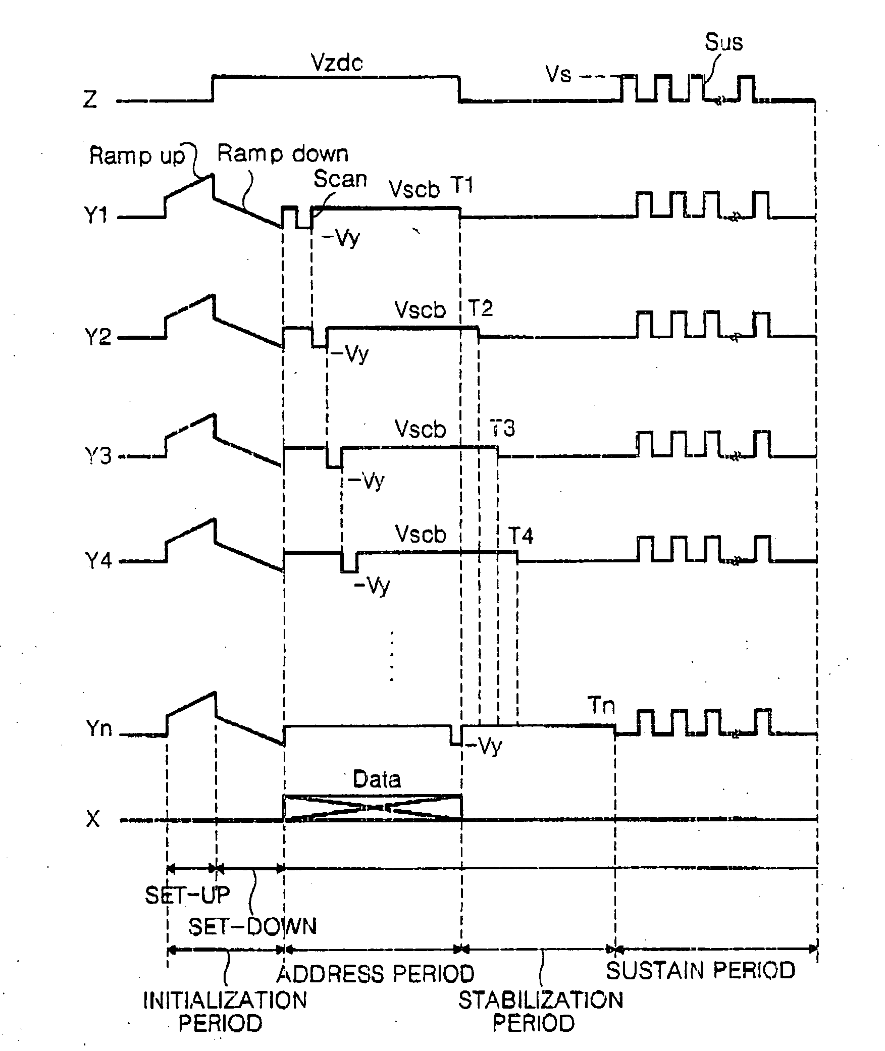
[0050]FIG. 7 is a waveform diagram for explaining a method of driving a plasma display panel according to the present invention.

[0051] In FIG. 7, Y represents the scan electrode; Z does the sustain electrode; and X does the address electrode.

[0052] Referring to FIG. 7, the PDP according to the first embodiment of the present invention is divided into an initialization period for initializing the full field, an address period for selecting a cell, an stabilization period for stably driving the PDP and a sustain period for sustaining a discharge of the selected cell for its driving.

[0053] In the initialization period, a rising ramp waveform Ramp-up is simultaneously applied to all the scan electrodes Y1 to Yn in a set-up interval. This rising ramp waveform Ramp-up causes a weak discharge within cells at the full field to generate wall charges within the cells. In the set-down interval, after the rising ramp waveform Ramp-up was supplied, a falling ramp waveform Ramp-down falling fro...

second embodiment

[0077]FIG. 12 is a waveform diagram for explaining a method of driving a plasma display panel according to the present invention.

[0078] In FIG. 12, Y represents the scan electrode; Z does the sustain electrode; and X does the address electrode.

[0079] Referring to FIG. 12, the PDP according to the second embodiment of the present invention is divided into an initialization period for initializing the full field, an address period for selecting a cell, an stabilization period for stably driving the PDP and a sustain period for sustaining a discharge of the selected cell for its driving.

[0080] In the initialization period, a rising ramp waveform Ramp-up is simultaneously applied to all the scan electrodes Y1 to Yn in a set-up interval. This rising ramp waveform Ramp-up causes a weak discharge within cells at the full field to generate wall charges within the cells. In the set-down interval, after the rising ramp waveform Ramp-up was supplied, a falling ramp waveform Ramp-down failing...


PUM


Abstract

A method and apparatus for driving a plasma display panel for preventing a generation of over current in the panel are disclosed. In the method, a scanning pulse falling from a first voltage is sequentially applied to a plurality of scan electrodes, and a data pulse is simultaneously applied to a plurality of address electrodes to select a cell. Said first voltage on the scan electrodes is lowered into a second voltage after said scanning pulse was applied to the scan electrodes in the last line. A time when said first voltage is lowered into said second voltage is controlled differently at any at least one of the scan electrodes.

Description

[0001] This application claims the benefit of Korean Patent Application No. P2003-59505 filed in Korea on Aug. 27, 2003, which is hereby incorporated by reference. BACKGROUND OF THE INVENTION [0002] 1. Field of the Invention [0003] This invention relates to a plasma display panel, and more particularly to a method and apparatus for driving a plasma display panel that is adaptive for preventing a generation of over current in the panel. [0004] 2. Description of the Related Art [0005] Generally, a plasma display panel (PDP) excites and radiates a phosphorus material using an ultraviolet ray generated upon discharge of an inactive mixture gas such as He+Xe, Ne+Xe or He+Ne+Xe, to thereby display a picture. Such a PDP is easy to be made into a thin-film and large-dimension type. Moreover, the PIMP provides a very improved picture quality owing to a recent technical development. [0006] Referring to FIG. 1, a discharge cell of a conventional three-electrode, AC surface-discharge PDP includ...

Claims


Application Information

Patent Timeline
IPC IPC(8): G09G3/288G09G3/20G09G3/291G09G3/293G09G3/298H01J17/49
CPCG09G3/2932G09G3/294G09G2330/025G09G2310/0218G09G2310/0267G09G3/296
Inventor LOH, JAE HYUN
Owner LG ELECTRONICS INC
Why Eureka
Try Eureka