Semiconductor structure and method for forming the same

a technology of semiconductors and structures, applied in the field of semiconductor manufacturing, can solve the problems of reducing the distance between a source and a drain of the device, and the possibility of subthreshold leakage, so as to improve the performance of the finfet, prevent stress relief in the fin, and improve the mobility of the carrier channel

Active Publication Date: 2022-06-23
SEMICONDUCTOR MANUFACTURING INTERNATIONAL (BEIJING) CORP +1
View PDF2 Cites 2 Cited by
  • Summary
  • Abstract
  • Description
  • Claims
  • Application Information

AI Technical Summary

Benefits of technology

[0027]According to forms of a method for forming a semiconductor structure provided in the present disclosure, the gate structure in the isolation region is removed to form an isolation opening, and first ion-doping is performed on the fin under the isolation opening to form an isolation doped region in the fin, a doping type of the isolation doped region being different from a doping type of the source-drain doping region. Therefore, a doping concentration of inversion ions in the fin of the isolation region can be increased, and a barrier of a P-N junction formed by the source-drain doping region and the fin of the isolation region can be increased accordingly, to prevent the device from generating a conduction current in the fin of the isolation region during operation, thereby implementing isolation between the fin of the isolation region and the fin of other regions through ion doping. Moreover, in embodiments and implementations of the present disclosure, there is no need to perform a fin cut process. Hence the fin is correspondingly made into a continuous structure, which helps prevent stress relief in the fin, thereby helping to improve carrier mobility of a channel. In summary, embodiments and implementations of the present disclosure help improve the performance of the FinFET.
[0028]Forms of a semiconductor structure of the present disclosure includes an isolation doped region, located in the fin of the isolation region, a doping type of the isolation doped region being different from a doping type of the source-drain doping region. Therefore, a doping concentration of inversion ions in the fin of the isolation region can be increased, and a barrier of a P-N junction formed by the source-drain doping region and the fin of the isolation region can be increased accordingly, to prevent the device from generating a conduction current in the fin of the isolation region during operation, thereby implementing isolation between the fin of the isolation region and the fin of other regions. Moreover, in embodiments and implementations of the present disclosure, isolation between the fin of the isolation region and the fin of other regions can be implemented without a fin cut process. Hence the fin is correspondingly made into a continuous structure, which helps prevent stress relief in the fin, thereby helping improve carrier mobility of a channel. In summary, embodiments and implementations of the present disclosure help improve the performance of the FinFET.

Problems solved by technology

However, as a channel length of a device becomes smaller, a distance between a source and a drain of the device also correspondingly decreases.
Therefore, a channel control capability of a gate structure deteriorates, and it is increasingly difficult to pinch off the channel by a gate voltage, resulting in a higher possibility of subthreshold leakage, that is, the so-called short-channel effect (SCE).

Method used


Image

  • Semiconductor structure and method for forming the same
  • Semiconductor structure and method for forming the same
  • Semiconductor structure and method for forming the same

Examples


Embodiment Construction

[0030]It can be known from the related art that a current performance of the FinFET still needs to be improved.

[0031]According to the analysis, taking a PMOS as an example, in a FinFET, SiGe is selected as the material of the fin, which can provide compressive stress to a channel of a PMOS device, thereby helping improve the carrier mobility.

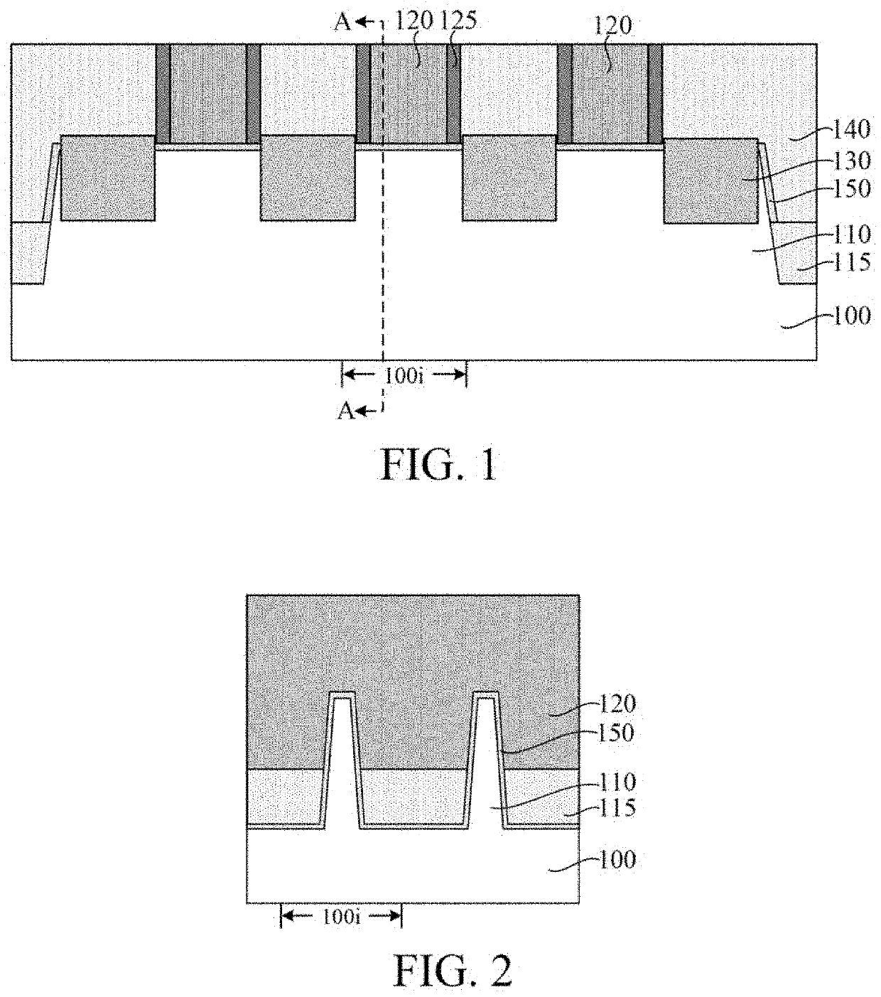
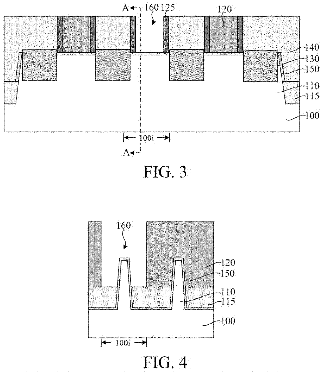
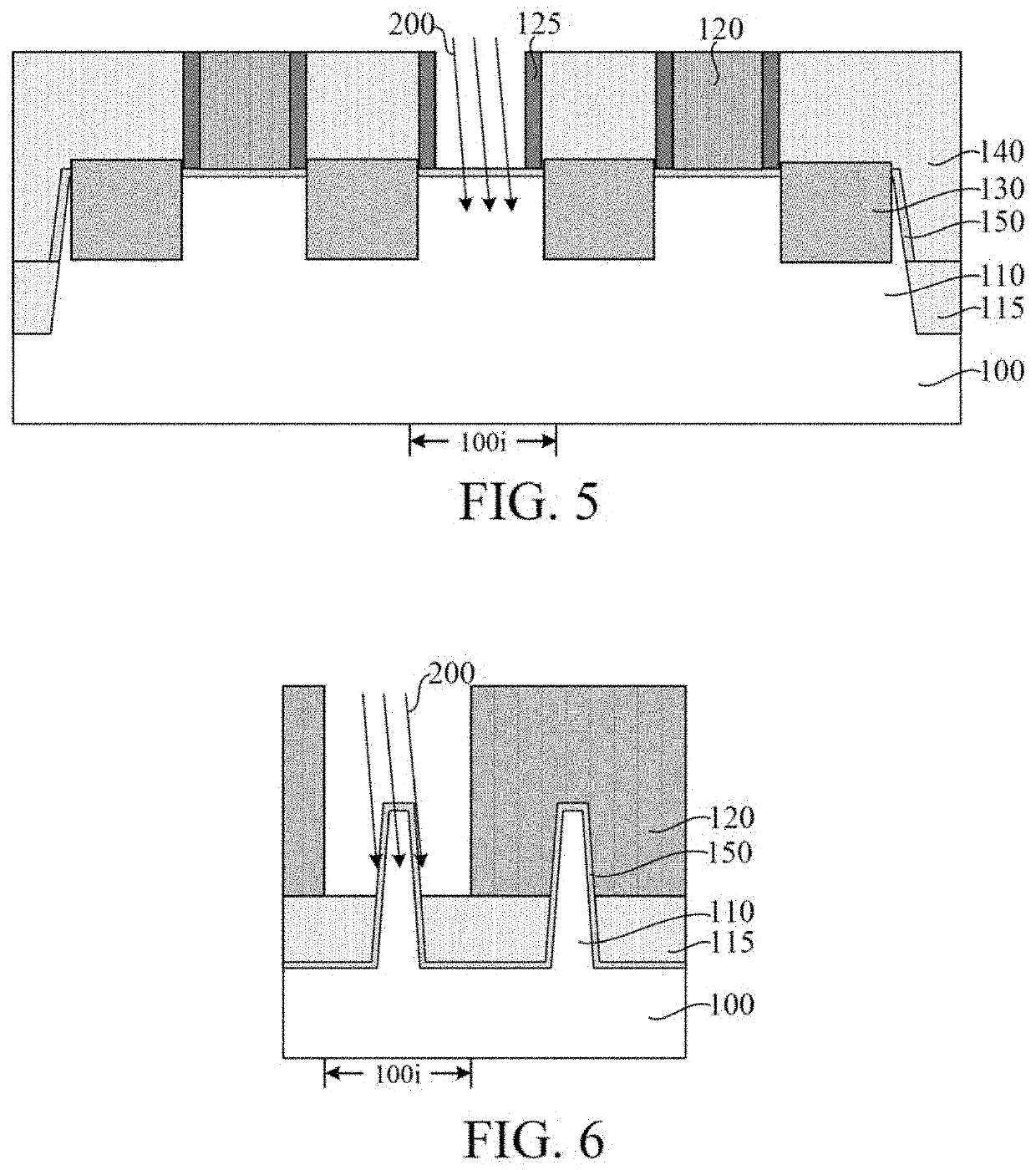
[0032]During the formation of a semiconductor structure, a fin cut process is usually also included. After fin is formed, the fin at an unnecessary position is cut away by a fin cut process. However, the fin cut process often leads to stress relief in the fin, which in turn leads to a poor effect of improving the carrier mobility.

[0033]One method is to cut away fin at an unnecessary position after a dummy gate structure, a source-drain doping region in the fin on both sides of the dummy gate structure, and an interlayer dielectric layer are formed.

[0034]This approach can alleviate the problem of stress relief in the fin, but the fin cut process ...


PUM

PropertyMeasurementUnit
temperatureaaaaaaaaaa

Abstract

A semiconductor structure and a method for forming the same are provided. In one form, a forming method includes: providing a base, a gate structure, a source-drain doping region, and an interlayer dielectric layer; removing the gate structure located in an isolation region to form an isolation opening and expose the top and side walls of a fin located in the isolation region; performing first ion-doping on the fin under the isolation opening to form an isolation doped region, a doping type of the isolation doped region being different from a doping type of the source-drain doping region; and filling the isolation opening with an isolation structure after the doping, the isolation structure straddling the fin of the isolation region. In embodiments and implementations of the present disclosure, the isolation doped region is formed, a doping concentration of inversion ions in the fin of the isolation region can thus be increased, and a barrier of a P-N junction formed by the source-drain doping region and the fin of the isolation region can be increased accordingly, to prevent the device from generating a conduction current in the fin of the isolation region during operation, thereby implementing isolation between the fin of the isolation region and the fin of other regions. Moreover, there is no need to perform a fin cut process. Hence the fin is made into a continuous structure, which helps prevent stress relief in the fin.

Description

RELATED APPLICATIONS[0001]The present application claims priority to Chinese Patent Appin. No. 202011510689.4, filed Dec. 18, 2020, the entire disclosure of which is hereby incorporated by reference.BACKGROUNDTechnical Field[0002]Embodiments and implementations of the present disclosure relate to the field of semiconductor manufacturing, and in particular, to a semiconductor structure and a method for forming the same.Related Art[0003]In semiconductor manufacturing, with the development of very-large-scale integrated circuits, a feature size of integrated circuits is continuously decreasing. To adapt to a smaller feature size, a channel length of a metal-oxide-semiconductor field-effect transistor (MOSFET) is also reduced. However, as a channel length of a device becomes smaller, a distance between a source and a drain of the device also correspondingly decreases. Therefore, a channel control capability of a gate structure deteriorates, and it is increasingly difficult to pinch off ...

Claims


Application Information

Patent Timeline
Patent Type & Authority Applications(United States)
IPC IPC(8): H01L29/66H01L29/78H01L21/8234
CPCH01L29/66795H01L21/823481H01L21/823431H01L29/7851H01L27/0886H01L21/823412H01L21/823493H01L21/823437H01L29/7848
Inventor OH, HANSULI, PENGCHONGSHI, XUEJIECHEN, YIYUSU, BO
Owner SEMICONDUCTOR MANUFACTURING INTERNATIONAL (BEIJING) CORP
Why Eureka
Try Eureka