Voltage generating circuit, semiconductor storage device and bit line charging method thereof

a voltage generation circuit and semiconductor technology, applied in static storage, digital storage, instruments, etc., can solve the problems of large voltage drop of the internal power supply voltage intvdd, excessive voltage level of the bit line, etc., to reduce the circuit area used for charging the bit line, power efficiency and peak current generation

Active Publication Date: 2020-12-17
WINBOND ELECTRONICS CORP
View PDF0 Cites 2 Cited by
  • Summary
  • Abstract
  • Description
  • Claims
  • Application Information

AI Technical Summary

Benefits of technology

[0021]According to the above description, the disclosure generates the charging voltages for charging the bit line from the first internal power supply voltage generated by using the external power supply voltage and selectively uses the charging voltage having the first driving capability and the charging voltage having the driving capability greater than the first driving capability to charge the bit line. In this way, compared to the prior art, the power efficiency and the peak current generated when charging the bit line are ameliorated, and a circuit area used for charging the bit line is reduced.

Problems solved by technology

However, if the adjustment is made by using the earliest condition of the charging period t1 of the external power supply voltage EXVDD, when the adjustment is applied to a device using the latest condition of the charging period t1 of the external power supply voltage EXVDD, at a point in time when the internal power supply voltage INTVDD is switched, a voltage level of the bit line becomes excessively low, which causes a large voltage drop of the internal power supply voltage INTVDD.

Method used


Image

  • Voltage generating circuit, semiconductor storage device and bit line charging method thereof
  • Voltage generating circuit, semiconductor storage device and bit line charging method thereof
  • Voltage generating circuit, semiconductor storage device and bit line charging method thereof

Examples


Embodiment Construction

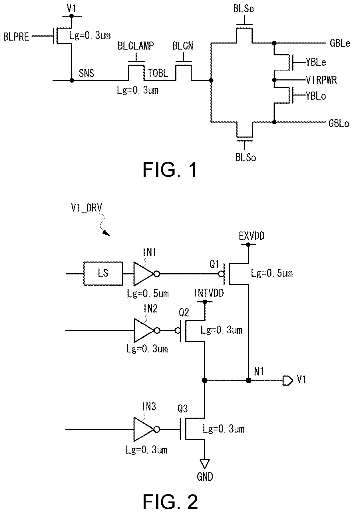
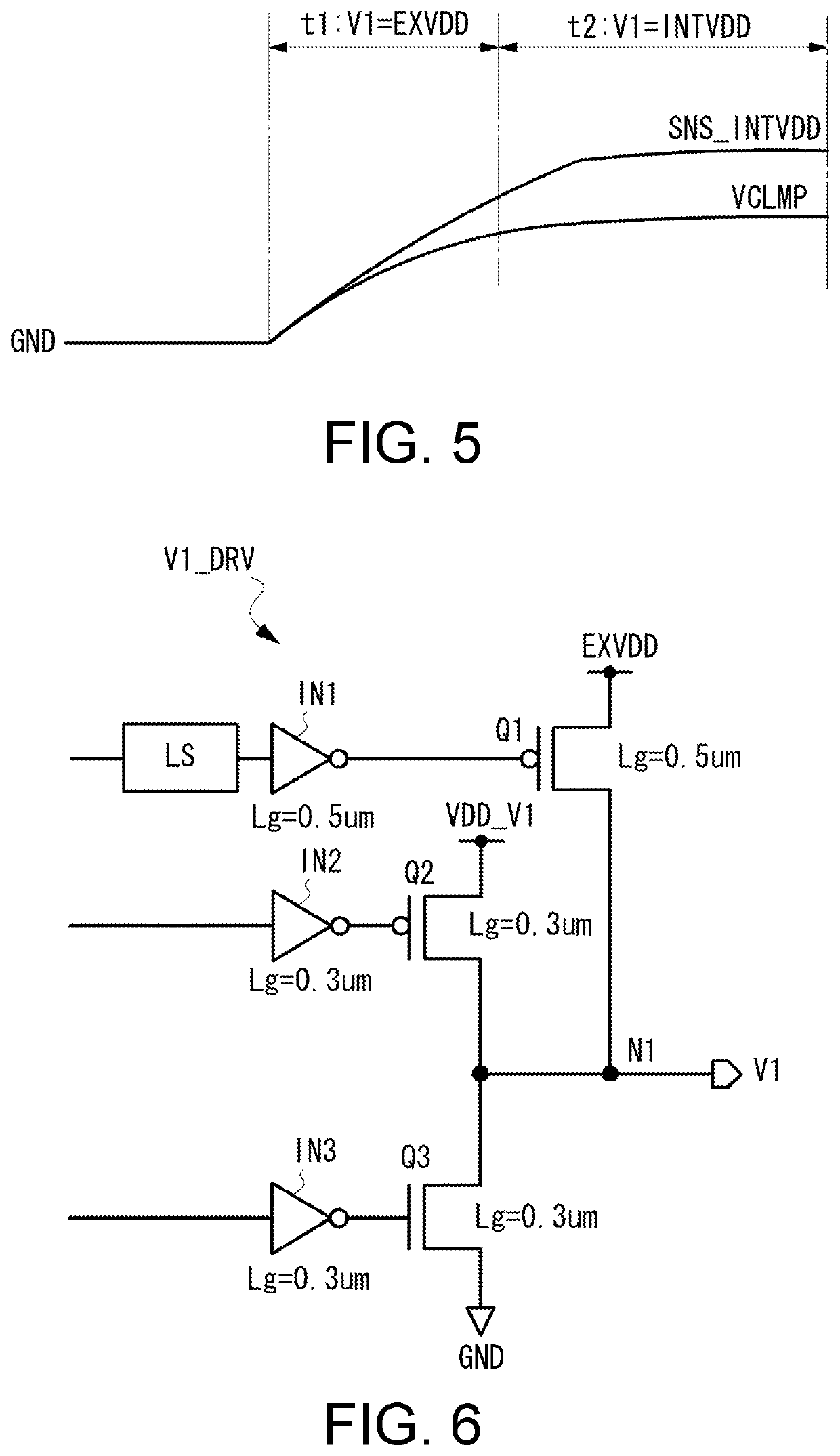
[0033]Generally, a NAND flash memory uses the driving circuit of the voltage V1 / the driving circuit of the virtual power supply VIRPWR when applying a voltage to a bit line. In the existing flash memory, in order to reduce a peak current, the external power supply voltage EXVDD is used when charging the bit line. Namely, after using the external power supply voltage EXVDD to charge the bit line during a fixed period, the external power supply voltage EXVDD is switched to the internal power supply voltage INTVDD for charging.

[0034]Since the existing driving circuit of the voltage V1 / the driving circuit of the virtual power supply VIRPWR (as shown in FIG. 6) uses the external power supply voltage EXVDD, components such as a level shifter LS, a low voltage P-type metal oxide semiconductor (low voltage PMOS, LVP) / low voltage N-type metal oxide semiconductor (low voltage NMOS, LVN) transistor with a gate length Lg=0.5 μm are required. Therefore, in order to protect the driving circuit of...


PUM

PropertyMeasurementUnit
voltage V1aaaaaaaaaa
lengthsaaaaaaaaaa

Abstract

A voltage generating circuit, a semiconductor storage device, and a bit line charging method thereof are provided. The voltage generating circuit includes: an INTVDD generating circuit for generating an internal power supply voltage INTVDD from an external power supply voltage EXVDD; a VDD_V1 generating circuit for generating an internal power supply voltage VDD_V1 from the external power supply voltage EXVDD; and a V1_driving circuit generating a charging voltage for charging the bit line at an output node by using the internal power supply voltage VDD_V1. The V1_driving circuit may generate voltages V1 having different driving capability. The V1_driving circuit charges the bit line with the voltage V1 having a weak driving capability during a first charging period of the bit line and charges the bit line with the voltage V1 having a strong driving capability during a second charging period.

Description

CROSS-REFERENCE TO RELATED APPLICATION[0001]This application claims the priority benefit of Japan application serial no. 2019-111694, filed on Jun. 17, 2019. The entirety of the above-mentioned patent application is hereby incorporated by reference herein and made a part of this specification.BACKGROUNDTechnical Field[0002]The disclosure relates to a semiconductor storage device such as a flash memory, etc., and particularly relates to suppression of a peak current during operation.Description of Related Art[0003]In a reading operation of a NAND flash memory, pages including even-numbered bit lines or pages including odd-numbered bit lines are alternately read. During a process of reading the even-numbered pages, the odd-numbered pages are cut off from a sense amplifier and a shield potential is supplied thereto, and during a process of reading the odd-numbered pages, the even-numbered pages are cut off from the sense amplifier, and the shield potential is supplied thereto, thereby ...

Claims


Application Information

Patent Timeline
Patent Type & Authority Applications(United States)
IPC IPC(8): G11C7/12G11C5/14
CPCG11C5/147G11C7/12G11C16/24G11C16/30G11C16/26G11C7/02G11C7/18G11C16/10
Inventor OKABE, SHO
Owner WINBOND ELECTRONICS CORP
Why Eureka
Try Eureka