Strained dislocation-free channels for CMOS and method of manufacture

a technology of dislocation-free channels and cmos, which is applied in the direction of electrical equipment, semiconductor devices, connection contact material, etc., can solve the problems of higher cost, disadvantageous to the performance of pfet, and beneficial to the performance of an n

Inactive Publication Date: 2005-04-21
IBM CORP
View PDF88 Cites 32 Cited by
  • Summary
  • Abstract
  • Description
  • Claims
  • Application Information

AI Technical Summary

Benefits of technology

[0011] In still a further aspect of the invention, a semiconductor structure includes a pFET and NFET channel formed in a substrate such as, for example, a Si layer. A shallow trench isolation structure is formed in the Si layer and a first layer of material in the pFET channel having a lattice constant different than the lattice constant of the Si layer. A second layer of material in the NFET channel has a lattice constant different than the lattice constant of the Si layer. An epitaxial semiconductor layer formed over the first layer of material in the pFET channel and the second layer of material in the NFET channel has substantially a same lattice constant as the Si layer thus creating a desired stress component within the pFET channel and the NFET channel.

Problems solved by technology

However, the same stress component, either tensile stress or compressive stress, discriminatively affects the characteristics of an n-type device and a p-type device.
That is, because the type of stress which is beneficial for the performance of an nFET is generally disadvantageous for the performance of the pFET.
While these methods do provide structures that have tensile stresses being applied to the NFET device and compressive stresses being applied along the longitudinal direction of the pFET device, they may require additional materials and / or more complex processing, and thus, resulting in higher cost.

Method used


Image

  • Strained dislocation-free channels for CMOS and method of manufacture
  • Strained dislocation-free channels for CMOS and method of manufacture
  • Strained dislocation-free channels for CMOS and method of manufacture

Examples


Embodiment Construction

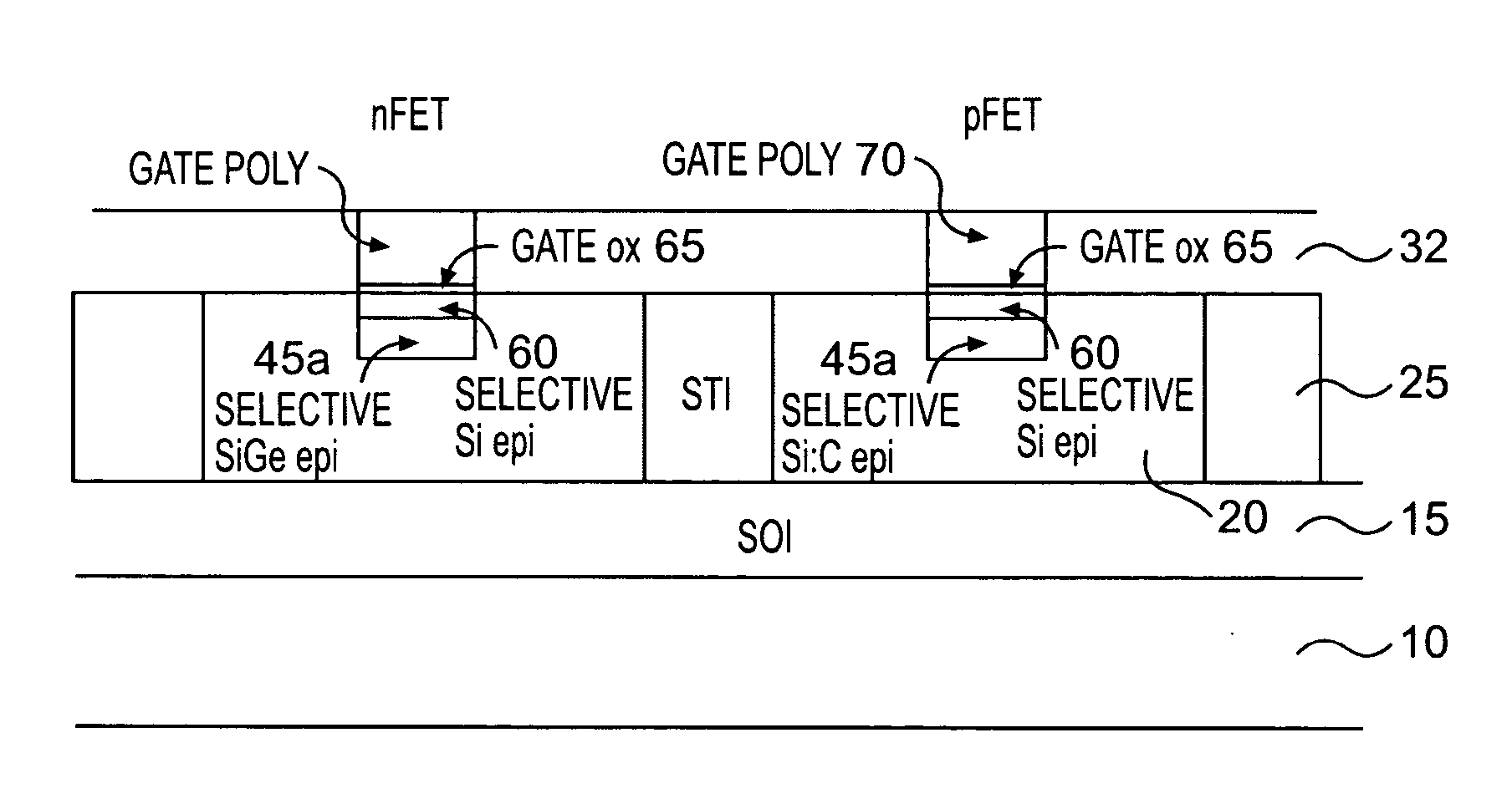
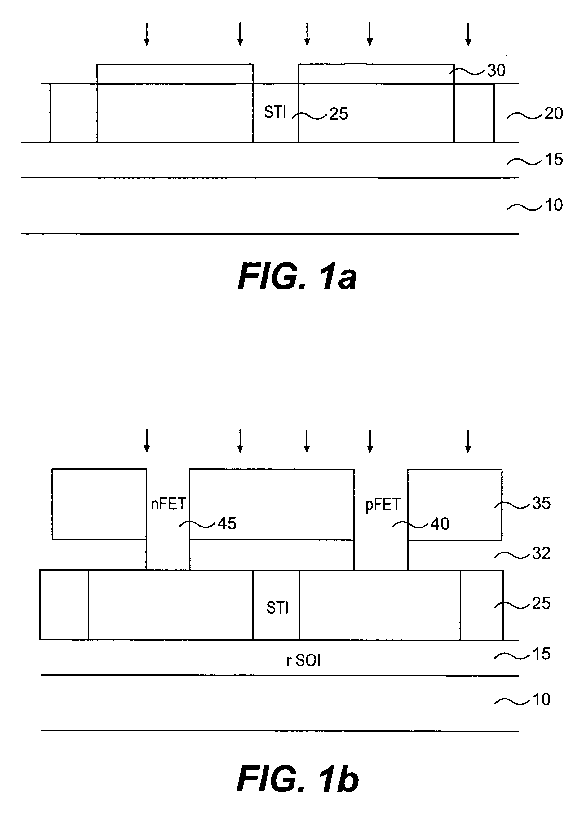
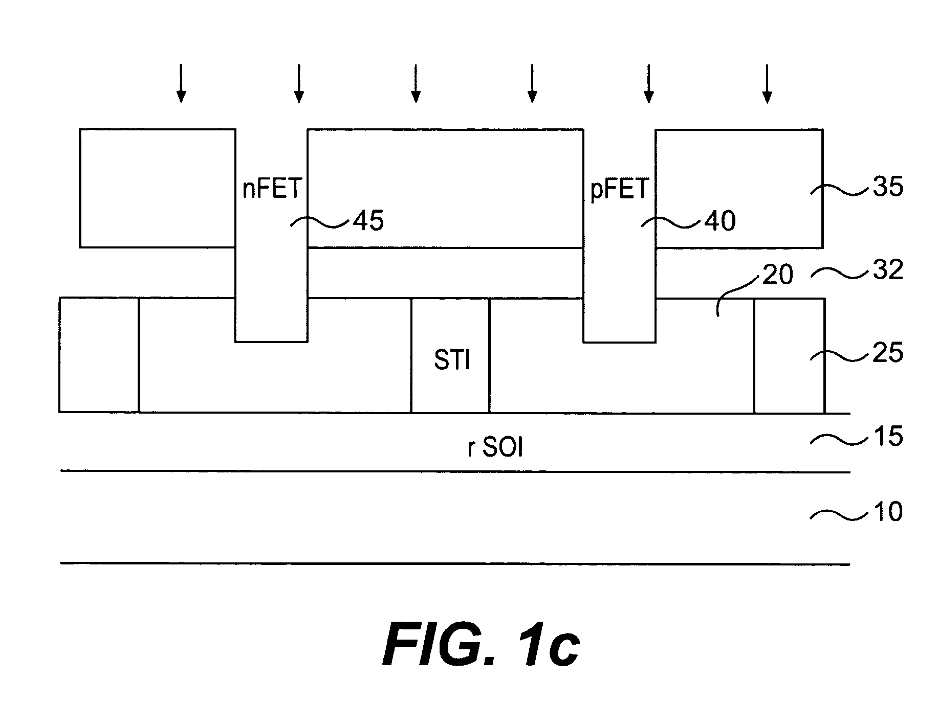
[0016] This invention is directed to a semiconductor device and method of manufacture which provides tensile stresses in the NFET channel and compressive stresses in the pFET channel of CMOS devices. In one embodiment, high tensile stresses may also be provided in the pFET channel to increase device performance. In one embodiment of the invention, channels are formed in the silicon layer in the area of the formation of the nFETs and pFETs. The channels are then filled with silicon based material having a naturally occurring lattice constant which does not match the lattice constant of the underlying silicon layer. By applying these materials, tensile and / or compressive forces result in an overlying epitaxial layer in the channels of the nFETs and pFETs, respectively. In one embodiment, the nFET and pFET channels can be formed simultaneously. By using the fabrication processes of the invention, improved device characteristics can be achieved, as well as higher yields and lower device...


PUM


Abstract

A semiconductor device and method of manufacturing a semiconductor device. The semiconductor device includes channels for a pFET and an NFET. An SiGe layer is grown in the channel of the NFET channel and a Si:C layer is grown in the pFET channel. The SiGe and Si:C layer match a lattice network of the underlying Si layer to create a stress component in an overlying grown epitaxial layer. In one implementation, this causes a compressive component in the pFET channel and a tensile component in the NFET channel. In a further implementation, the SiGe layer is grown in both the NFET and pFET channels. In this implementation, the stress level in the pFET channel should be greater than approximately 3 GPa.

Description

BACKGROUND OF THE INVENTION [0001] 1. Field of the Invention [0002] The invention generally relates to a semiconductor device and method of manufacture and, more particularly, to a semiconductor device and method of manufacture which imposes tensile and compressive stresses in the device during device fabrication. [0003] 2. Background Description [0004] Mechanical stresses within a semiconductor device substrate can modulate device performance. That is, stresses within a semiconductor device are known to enhance semiconductor device characteristics. Thus, to improve the characteristics of a semiconductor device, tensile and / or compressive stresses are created in the channel of the n-type devices (e.g., NFETs) and / or p-type devices (e.g., PFETs). However, the same stress component, either tensile stress or compressive stress, discriminatively affects the characteristics of an n-type device and a p-type device. [0005] In order to maximize the performance of both nFETs and pFETs within...

Claims


Application Information

Patent Timeline
Patent Type & Authority Applications(United States)
IPC IPC(8): H01LH01L21/00H01L21/8238H01L21/84H01L27/12H01L29/04H01L31/036H01R4/64
CPCH01L21/823807H01L21/84Y10S438/933H01L29/1054H01L29/66621H01L27/1203H01L21/18H01L29/768H01L29/772
Inventor CHIDAMBARRAO, DURESETIDOKUMACI, OMER H.
Owner IBM CORP
Why Eureka
Try Eureka