Electronic component mounting apparatus and electronic component mounting method

a technology for mounting apparatuses and electronic components, applied in the direction of manufacturing tools, instruments, transportation and packaging, etc., can solve the problems of increasing the size of the total of the apparatus, difficulty in promoting an operational efficiency, and difficulty in manual handling of background art, etc., to achieve excellent operational efficiency

Inactive Publication Date: 2005-04-28
PANASONIC CORP
View PDF7 Cites 6 Cited by
  • Summary
  • Abstract
  • Description
  • Claims
  • Application Information

AI Technical Summary

Benefits of technology

[0007] Hence, it is an object of the invention to provide a compact electronic component mounting apparatus and an electronic component mounting method excellent in an operational efficiency. Particularly, it is provided an electronic component mounting apparatus and an electronic component mounting method capable of realizing a mechanism of interchanging a component holding jig of a wafer ring or the like by a compact constitution.

Problems solved by technology

However, according to the electronic component mounting apparatus of the background art, the interchanging apparatus provided separately is constituted to attach to the electronic component mounting apparatus and therefore, along with a problem in view of arranging a facility in which large-sized formation of a total of the facility is unavoidable, a time lag in operation is unavoidable for avoiding interference between operation of recognizing a component by a component recognizing camera and operation of interchanging the wafer ring and there is a case in which it is difficult to promote an operational efficiency.
Therefore, a size and a weight of a magazine containing a number of sheets of semiconductor wafers are increased, manual handling of the background art becomes difficult and therefore, there is adopted a method of mounting a magazine to an electronic component mounting apparatus by exclusive handling means of a carriage or the like.
However, according to the background art described in JP-A-10-270532 or U.S. Pat. No. 5,839,187, when a mechanism of carrying in and carrying out a wafer ring to interchange is attached to the electronic component mounting apparatus, it is difficult to compactly realize a constitution suitable for access by the above-described exclusive handling means to pose a problem that the size of the total of the apparatus is increased.

Method used


Image

  • Electronic component mounting apparatus and electronic component mounting method
  • Electronic component mounting apparatus and electronic component mounting method
  • Electronic component mounting apparatus and electronic component mounting method

Examples


embodiment 1

(Embodiment 1)

[0020] An embodiment of the invention will be explained with reference to the drawing as follows.

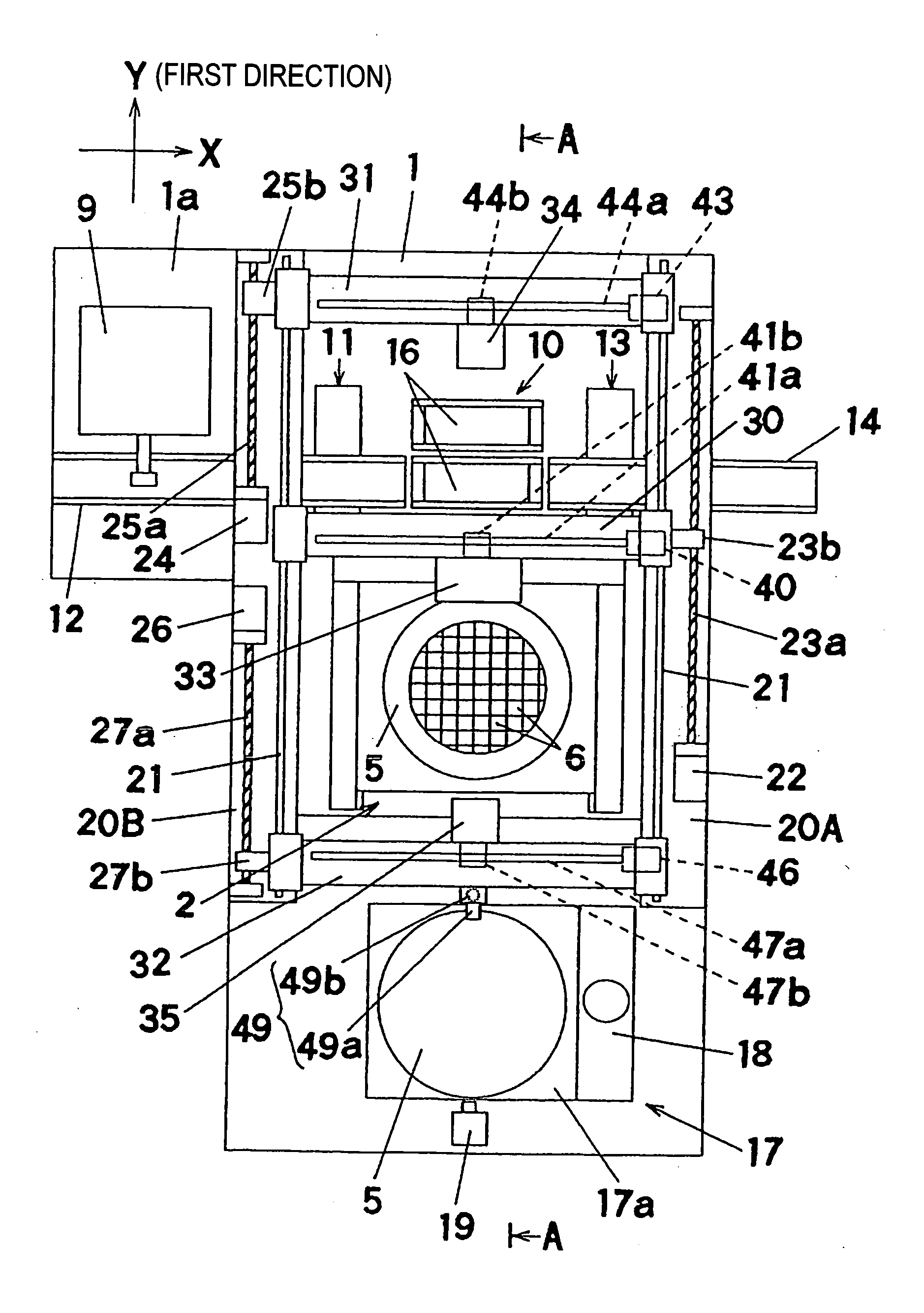
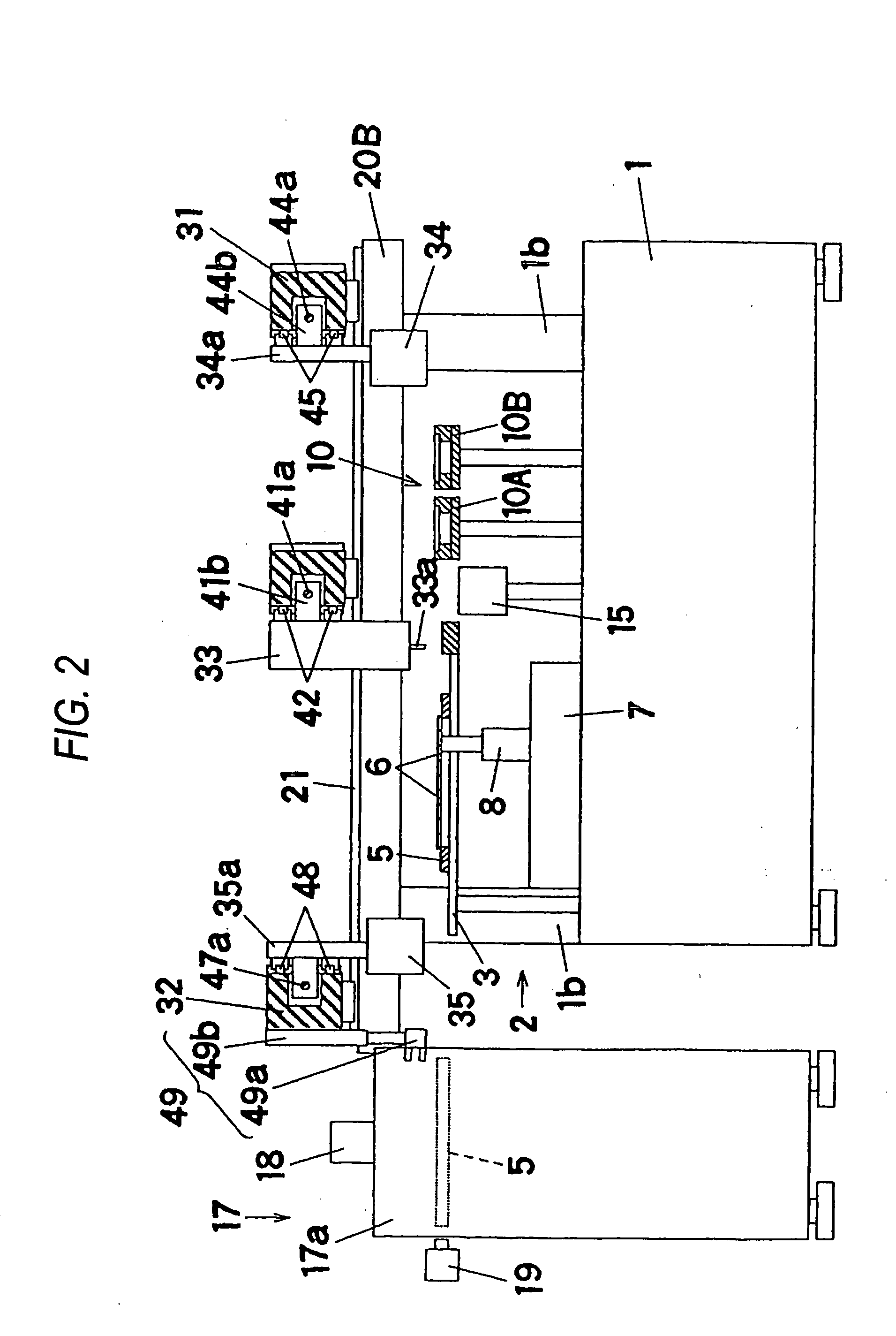
[0021] An explanation will be given of a total structure of an electronic component mounting apparatus with reference to FIG. 1 and FIG. 2. FIG. 2 shows a section taken along a line A-A of FIG. 1. In FIG. 1, an electronic component supply portion 2 is arranged on a base 1. As shown by FIG. 2, the electronic component supply portion 2 is provided with a wafer holding table 3, and the wafer holding table 3 detachably holds a wafer ring 5 which is a component holding jig. A sheet (illustration thereof is omitted) expanded to the wafer ring 5 is pasted with semiconductor chips 6 (hereinafter, abbreviated simply as “chip 6”) which are electronic components in a state of being separated to individual pieces thereof and in a state of holding the wafer ring 5 at the wafer holding table 3, the electronic component supply portion 2 supplies the chips 6 held by being aligned by a plu...

embodiment 2

(Embodiment 2)

[0063] Next, another embodiment of the invention will be explained in reference to the drawing.

[0064] First, an explanation will be given of a total structure of an electronic component mounting apparatus in reference to FIG. 7 and FIG. 8. FIG. 8 shows a section taken along line A-A of FIG. 7. In FIG. 7, a board carrying path 102 is arranged above a base 101 in X direction. The board carrying path 102 carries a board 103 mounted with an electronic component to an electronic component mounting position to position to hold. Therefore, the board carrying path 102 constitutes a board holding portion arranged at a position remote from an electronic component supply portion 104 in Y direction (first direction).

[0065] As shown by FIG. 8, the electronic component supply portion 104 is provided with a jig holder 107 and the jig holder 107 is detachably mounted with a wafer ring 105 for holding a sheet pasted with a semiconductor chip 106 (hereinafter, abbreviated simply as “c...


PUM

PropertyMeasurementUnit
sizeaaaaaaaaaa
sizeaaaaaaaaaa
weightaaaaaaaaaa

Abstract

Jig interchanging mechanism for supplying and carrying out a component holding jig to and from an electronic component supply portion is moved by a component image taking camera moving mechanism for moving the component image taking camera above the electronic component supply portion, the compact electronic component mounting apparatus and the electronic component mounting method excellent in an operational efficiency can be realized.

Description

BACKGROUND OF THE INVENTION [0001] The present invention relates to an electronic component mounting apparatus and an electronic component mounting method for mounting an electronic component on a circuit board. [0002] In a background art, an electronic component supplied in a state of a semiconductor wafer such as a semiconductor chip or the like is mounted onto a circuit board of lead frame or the like by an electronic component mounting apparatus having an exclusive supply apparatus. An adhering sheet pasted with the semiconductor wafer is mounted to the supply apparatus in a state of being held by a wafer ring and when all of semiconductor chips are taken out from a single wafer ring, the empty wafer ring is interchanged by a new wafer ring by an interchanging apparatus having a grabbing and carrying function. For example, it is proposed in Japanese Patent Publication JP-A-10-270532 or U.S. Pat. No. 5,839,187. [0003] Further, when the semiconductor chip is taken out from the adh...

Claims


Application Information

Patent Timeline
Patent Type & Authority Applications(United States)
IPC IPC(8): H01L21/00H05K13/02
CPCH01L21/67144Y10T29/53178H05K13/02B65G47/918H01L21/67721H01L21/67754H05K13/0404
Inventor YAKIYAMA, HIDEYUKIEMOTO, YASUHIRO
Owner PANASONIC CORP
Why Eureka
Try Eureka