Power switching cell with normally conducting field-effect transistors

a field-effect transistor and power switching technology, applied in the field of power switching, can solve the problems of increased switching time t, reduced current ids/sub>2, increased electrical losses in the off state, etc., and achieves the effect of simplifying control logic and improving switching speed

Active Publication Date: 2017-02-16
THALES SA +3
View PDF4 Cites 4 Cited by
  • Summary
  • Abstract
  • Description
  • Claims
  • Application Information

AI Technical Summary

Benefits of technology

[0031]This cell has various advantages, as explained in detail in the aforementioned application. In particular, the switching speed is improved, as a very small variation in the input voltage, of the order of a few millivolts in the vicinity of a threshold that depends on the two values of the resistors R1 and R2, is sufficient to obtain the transition of the cell. As a result, the control signal applied as input does not require precise shaping. The control logic is thereby simplified.
[0032]However, this cell necessitates a compromise between switching speed and electrical losses. Specifically, the self-biasing resistor R2 must respond to two contradictory constraints:
[0033]it is desirable for the value of this resistor R2 to be as high as possible when the power transistor T2 is in the OFF state. Specifically, in this OFF state, the source voltage of the power transistor is close to zero, without actually being zero. The higher the value of the resistor R2, the further the source voltage is pulled toward zero: consumption in the OFF state of the power transistor will be correspondingly lower.
[0034]it is desirable for the value of this resistor R2 to be as low as possible in order to favor high-speed switching of the transistor from the OFF state to the ON state;
[0035]specifically, high-frequency switching is sought. In this instance it involves minimizing the time constant τ=Cin2*R2 associated with the charge of the input capacitance C1n2 of the transistor T2, inherent to its technology. The input capacitance encompasses the gate-source capacitance of the transistor and the parasitic capacitances on the gate due to the Miller effect.
[0036]The effects linked to these two constraints appear clearly in FIGS. 2 to 4 which show the drain-source voltage (Vds2) and current (Ids2) curves of the transistor T2 as a function of time, obtained for various self-biasing resistor R2 values. The current curves are here shown as dotted lines and the voltage curves as continuous lines.

Problems solved by technology

Specifically, if the current Ids2 is too large, then the current through R2 will also be too large and the voltage Vds2 will also be too high, requiring the closure of T2 and therefore leading to a decrease in the current Ids2.
However, this cell necessitates a compromise between switching speed and electrical losses.
Thus, if the transistor T2 quickly switches from the ON state to the OFF state, electrical losses in the OFF state are actually increased.
However, the switching time t(ON->OFF) is much increased and is about 10 nanoseconds: the time constant linked to the input capacitance of the power transistor is too large.
Additionally, these losses contribute to adversely affecting the working life of the power transistor of these cells.
Thus, as very clearly shown in these figures, a problem with this cell structure is the necessary compromise to be struck between switching speed and electrical losses, through the choice of the value of the self-biasing resistor.
The cell described above has proven to be ill-suited to this type of application, using currently available transistor technologies.

Method used


Image

  • Power switching cell with normally conducting field-effect transistors
  • Power switching cell with normally conducting field-effect transistors
  • Power switching cell with normally conducting field-effect transistors

Examples


Embodiment Construction

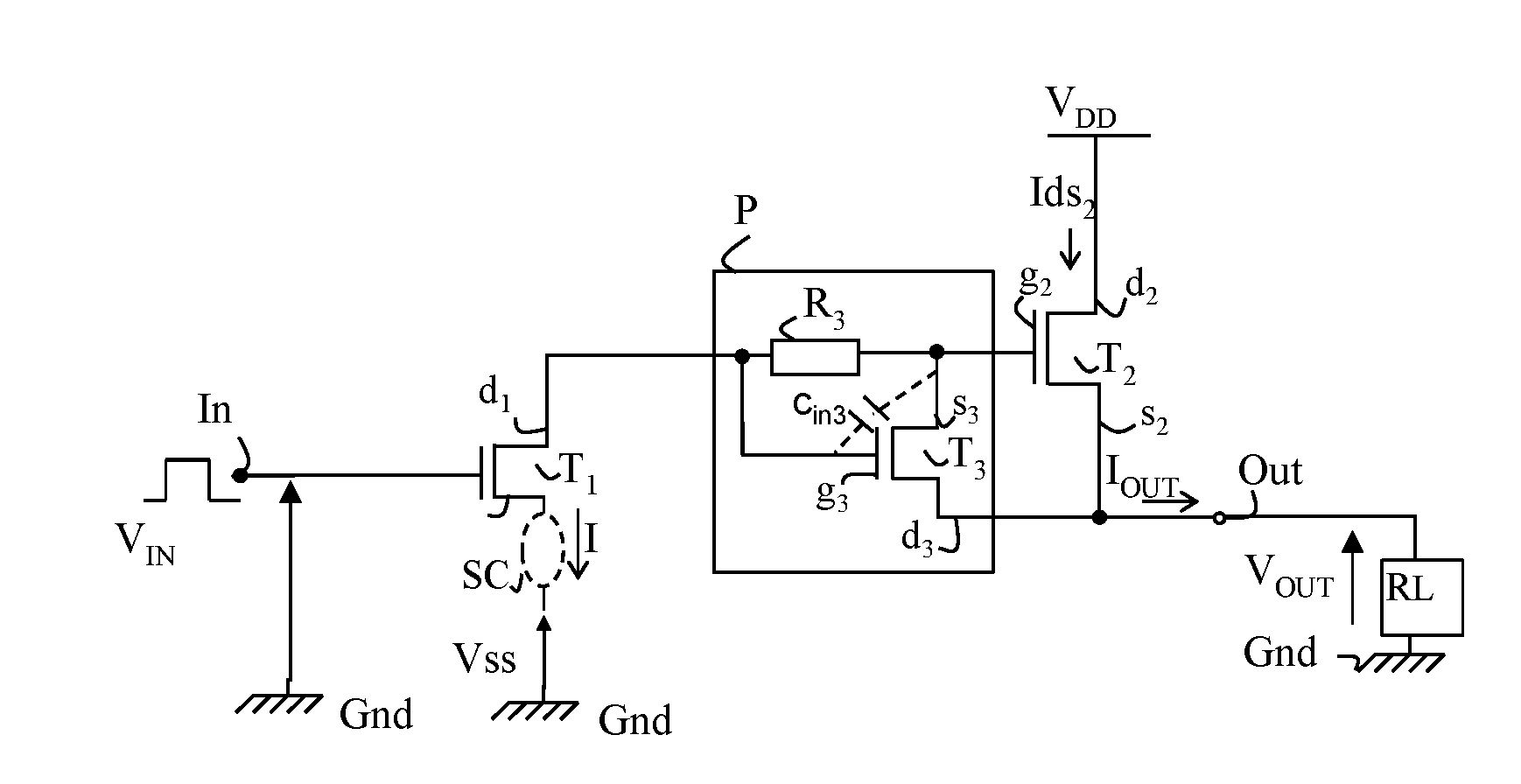
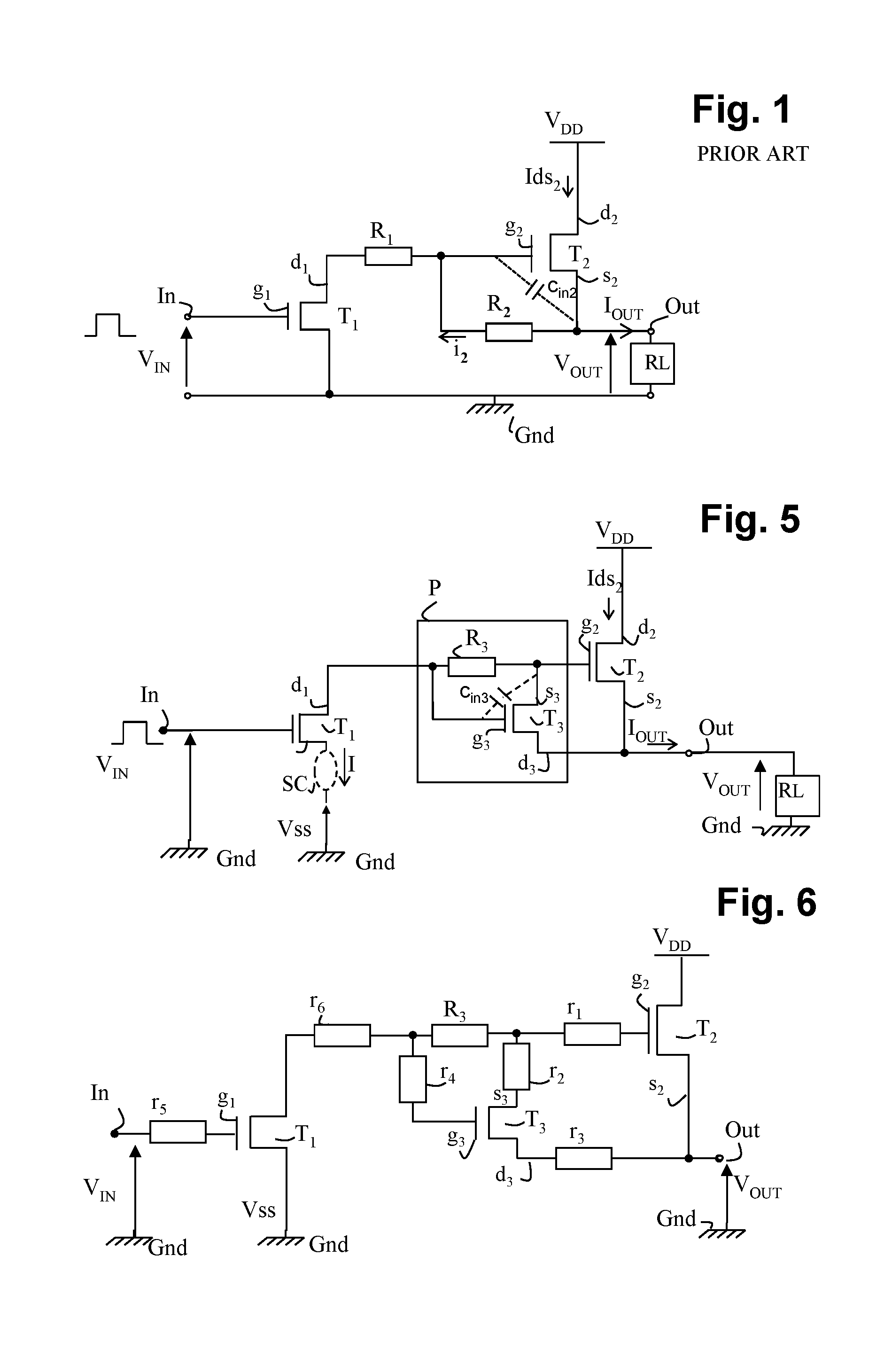
[0082]A basic structure of a cell according to the invention is illustrated in FIG. 5. For the sake of simplicity, the elements common to the cell of the prior art that is illustrated in FIGS. 1 to 4 and to the cell of the invention illustrated in FIGS. 5 to 13 bear the same references. The self-biasing and power transistors of the cell are normally on (ON state) field-effect transistors, even if this is not necessarily specified for the purpose of not overburdening the disclosure.

[0083]The basic structure of a cell according to the invention illustrated in FIG. 5 shares the current switch formed by the input transistor T1 and the power transistor T2 that switches the high voltage Vdd with the cell of the prior art illustrated in FIG. 1.

[0084]The self-biasing resistor R2 for biasing the gate of the power transistor of the cell of FIG. 1 is replaced, in the cell according to the invention, by a self-biasing circuit P for biasing the gate comprising:

[0085]a transistor T3 that is a nor...


PUM


Abstract

A power switching cell with normally on field-effect transistors comprises a current switch receiving the control input signal over an activation input and a power transistor for switching a high voltage VDD applied to its drain, to its source that is connected to the output port of the cell. The control of the gate of the power transistor whose source is floating, according to the input signal, is provided by a self-biasing circuit connected between its gate and source. The current switch is connected between the self-biasing circuit and a zero or negative reference voltage. The self-biasing circuit comprises a transistor whose source or drain is connected to the gate or source of the power transistor. The gate of this transistor is biased by a resistor connected between its gate and source, and between the current switch and the source. The transistors are HEMT transistors using GaN or AsGa technology.

Description

FIELD OF THE INVENTION[0001]The invention relates to power switching and, more particularly, power switching for radiofrequency applications. The field of application of the invention is particularly that of radar or wireless telecommunications systems.PRIOR ARTContext[0002]Telecommunications RF signals carry ever more information, coded by virtue of various types of modulation (OFDM, 16-QAM, etc.) that cause, in particular, large and rapid variations in their envelopes. Given the low electrical efficiencies of conventional RF amplifiers for amplifying these signals exhibiting complex modulations, various amplifier architectures have been proposed and developed that allow better electrical efficiencies of amplification to be obtained and a good level of linearity to be retained.[0003]One technique for improving the electrical efficiency of amplification consists particularly of dynamically managing the polarization of a radiofrequency amplifier according to the variations in the env...

Claims


Application Information

Patent Timeline
Patent Type & Authority Applications(United States)
IPC IPC(8): H03K17/687H03K17/041
CPCH03K17/04106H03K17/687H03K19/09407
Inventor JARDEL, OLIVIERQUERE, RAYMONDPIOTROWICZ, STEPHANEBOUYSSE, PHILIPPEDELAGE, SYLVAINMARTIN, AUDREY
Owner THALES SA
Why Eureka
Try Eureka