

Multiple gate semiconductor device and method for forming same
- Summary
- Abstract
- Description
- Claims
- Application Information
AI Technical Summary
Benefits of technology
Problems solved by technology
Method used
Image

Examples
Embodiment Construction
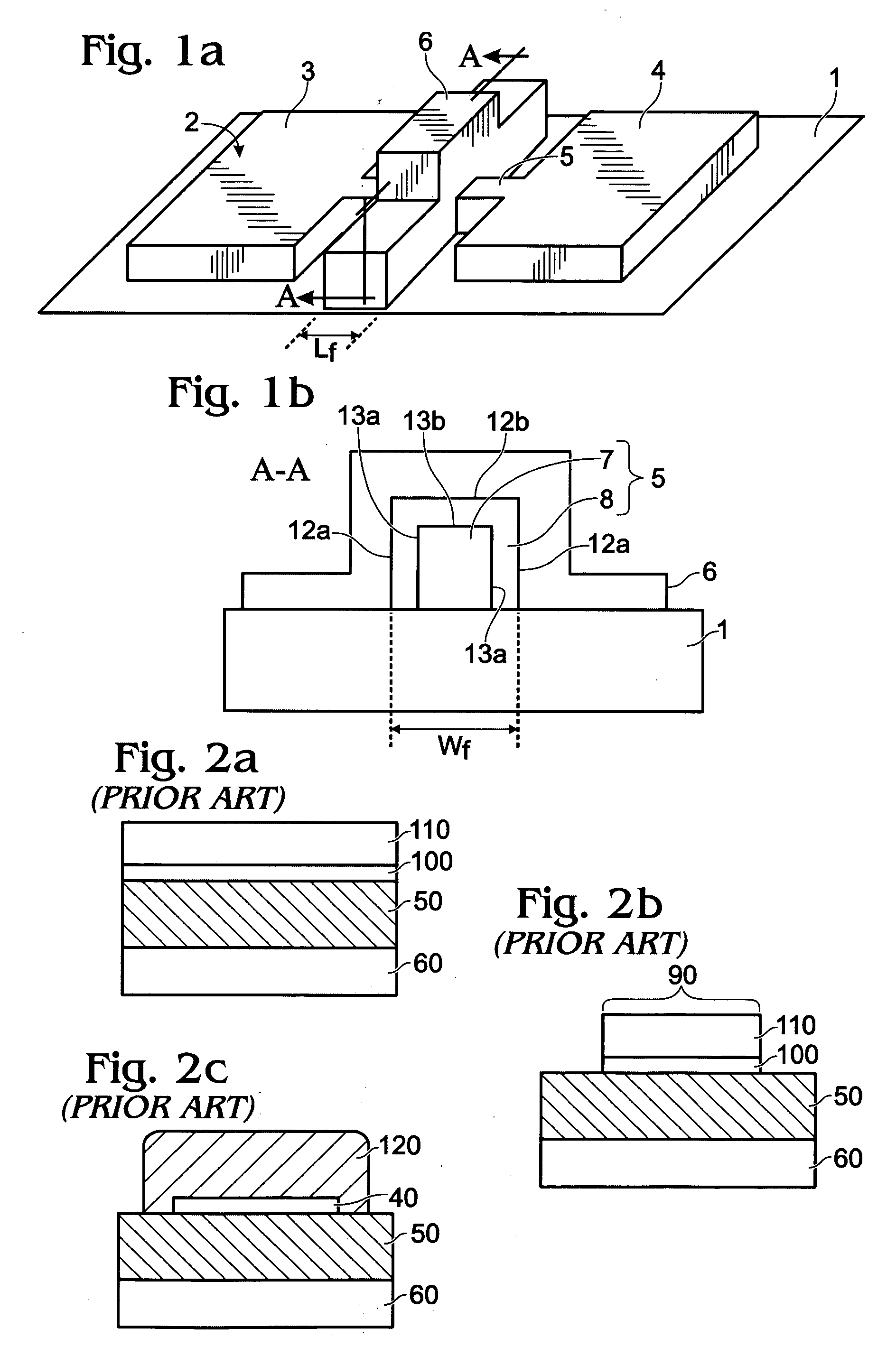
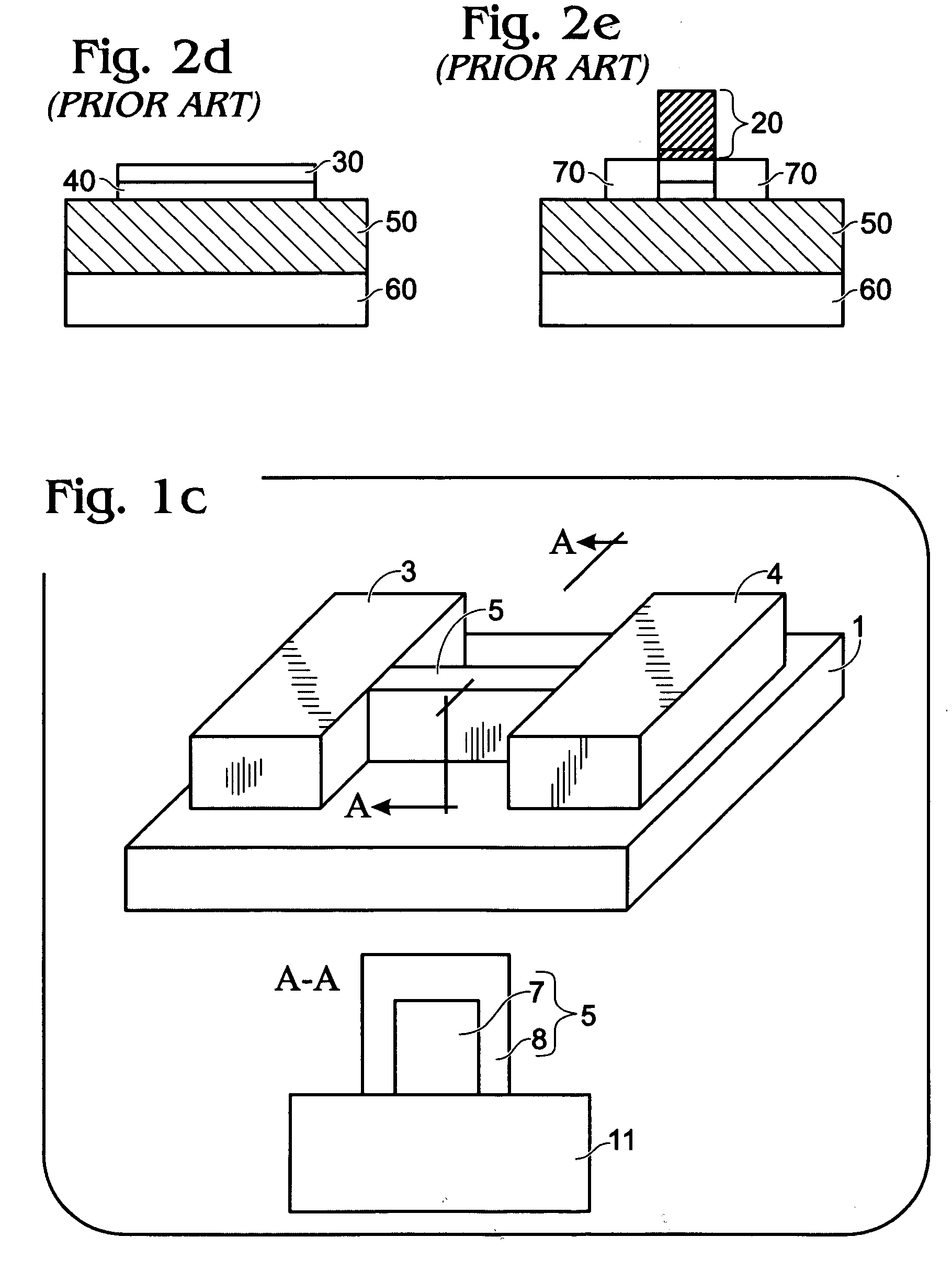
[0020] While embodiments of multiple gate semiconductor devices are generally discussed herein with respect to Fin Field Effect Transistors (FinFETs), it will be appreciated that the invention is not limited in this respect and that embodiments of the invention may be implemented in any number of types of device. For example, in his article “Beyond the Conventional Transistor”, published in IBM Journal of Research & Development, Vol. 46, No. 23 2002, which in incorporated by reference herein in it entirety, H. S. Wong discloses various types of multi-gate devices. In FIGS. 14, 15 and 17 of this paper, alternative orientations of double and triple-gate devices are depicted with the corresponding process sequences being detailed on pages 146-152 of that paper. Such device configurations may be employed with embodiments of the invention.
1. Improved FinFET Devices
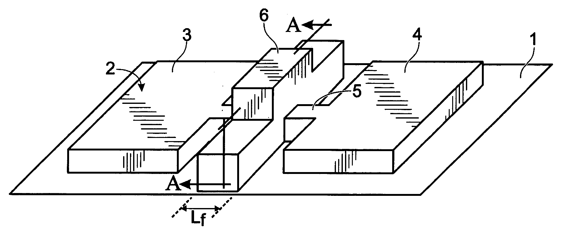
[0021] Referring now to FIG. 1, an improved semiconductor device is shown. The device of FIG. 1 may be referred to as a st...
PUM
 Abstract
Description
Claims
Application Information