Delay locked loop phase blender circuit

a delay lock and blender technology, applied in the direction of pulse manipulation, pulse automatic control, pulse technique, etc., can solve the problems of large number of inverters and comparators, large number of inverters and may consume a significant amount of current, and large delay time of units that are too coarse to provide the phase resolution required to adequately synchroniz

Inactive Publication Date: 2005-05-05
INFINEON TECH AG
View PDF7 Cites 89 Cited by
  • Summary
  • Abstract
  • Description
  • Claims
  • Application Information

AI Technical Summary

Benefits of technology

[0014] Embodiments of the present invention generally provide improved techniques and circuit configurations for the fine adjustment of a signal generate by a DLL circuit.
[0016] Another embodiment provides a phase blending circuit for generating a plurality of signals differing in phase relative to an early phase signal. The phase blending circuit generally includes a current source having a common output node and a control input for disabling the current source when a late phase signal trailing the early phase signal is asserted, a comparator having an input coupled with the common output node of the current source, a plurality of delay elements, a path for current flow from the common output node when the early phase signal is asserted, and a plurality of switches to selectively couple one or more of the delay elements to the output node of the current source for varying the time required for a voltage level of the common output node to fall below a threshold level as a result of current flow through the path.

Problems solved by technology

Unfortunately, this unit delay time may be too coarse (large) to provide the phase resolution required to adequately synchronize CKIN and CKOUT for high speed applications.
For example, determining the sizes of blending inverters with adequate precision to generate phase signals having a desired resolution can be a difficult task.
As a result, the large number of inverters and comparators may consume a significant amount of current.

Method used


Image

  • Delay locked loop phase blender circuit
  • Delay locked loop phase blender circuit
  • Delay locked loop phase blender circuit

Examples


Embodiment Construction

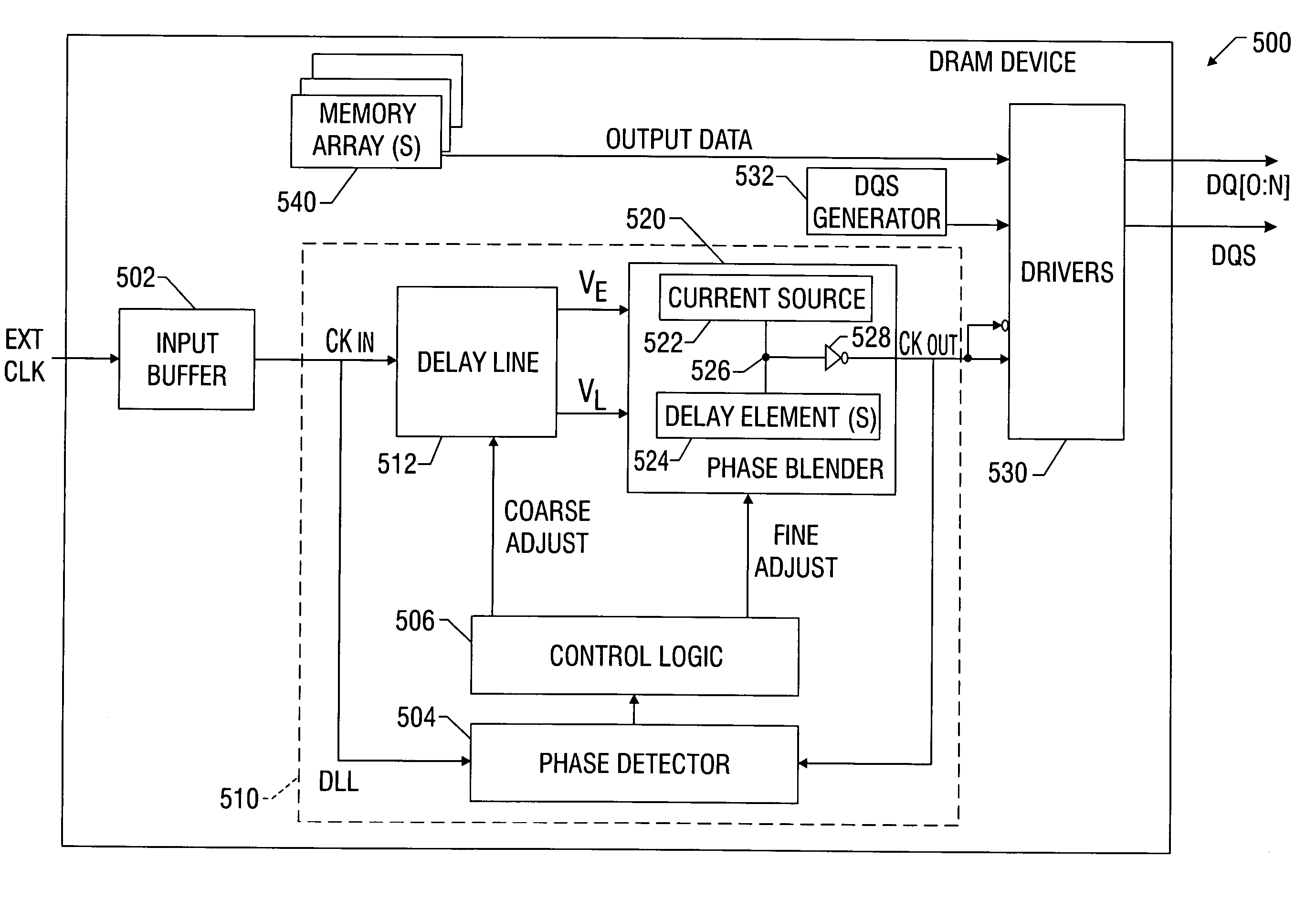
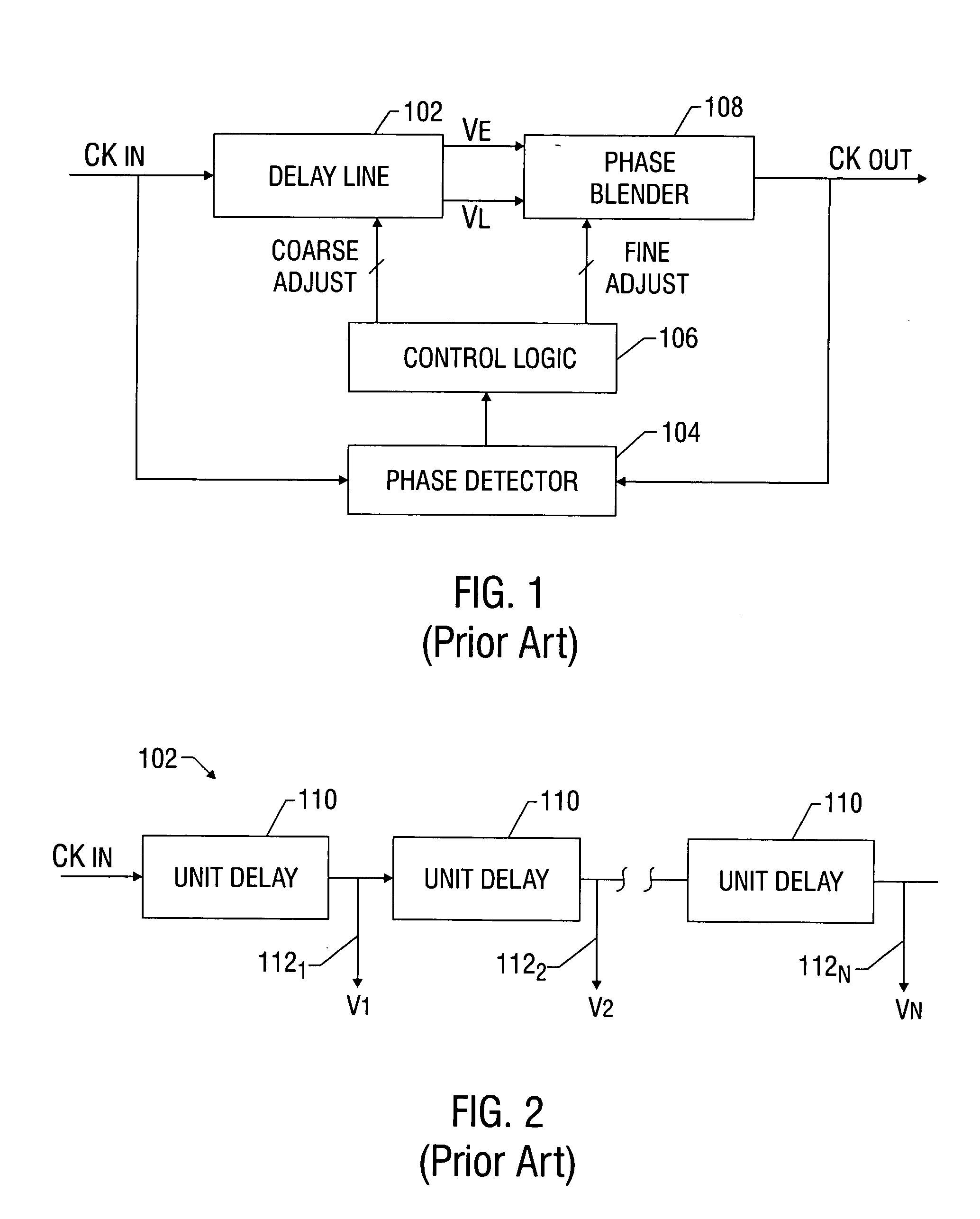
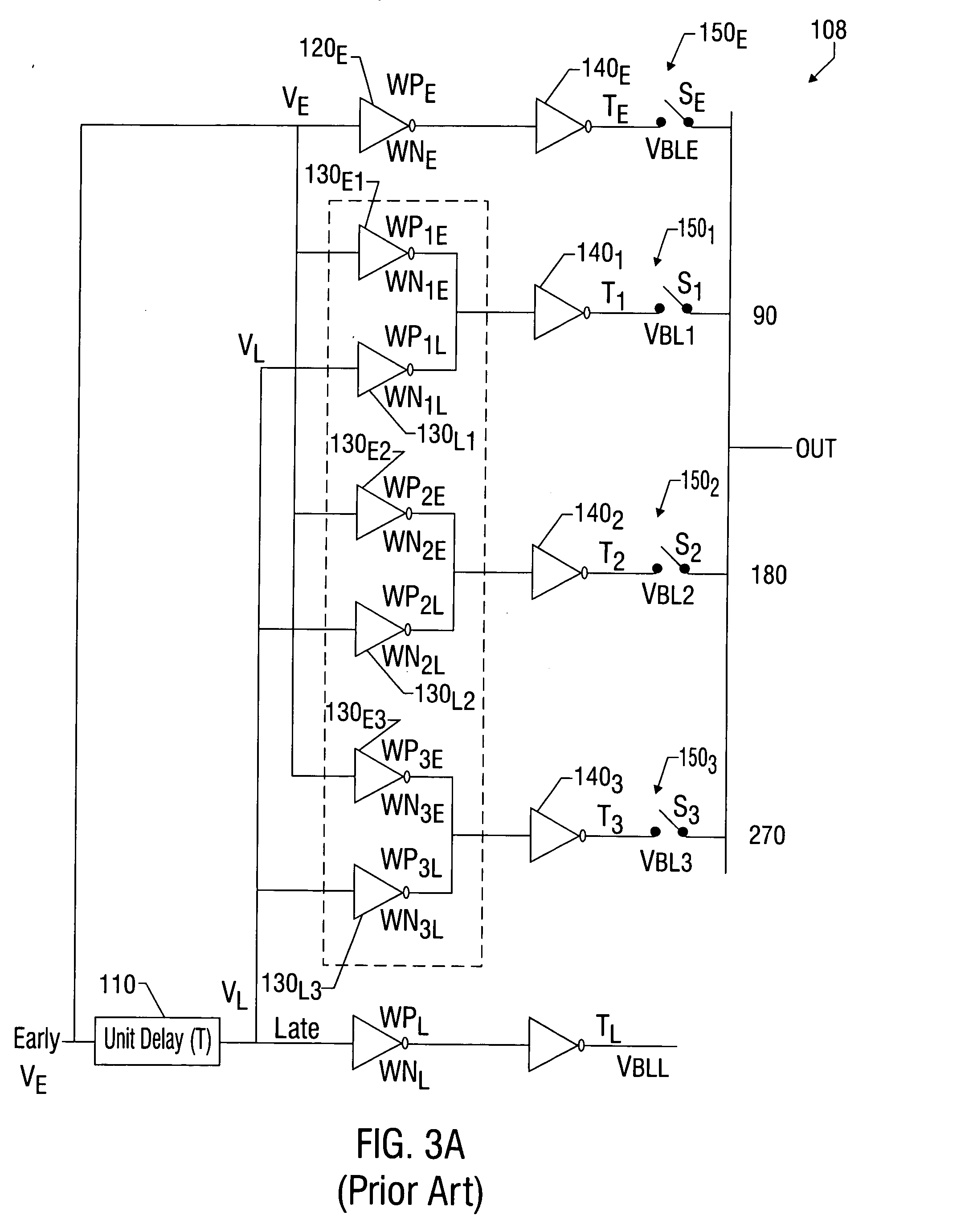
[0031] Embodiments of the present invention generally provide improved techniques and circuit configurations for fine phase adjustments, for example, in a delay-locked loop (DLL) circuit. Rather than utilize one or more different current sources to generate each fine adjust phase signal as in the prior art (e.g., the transistors PE and PL in each pair of blending inverters 130 of FIG. 1), embodiments of the present invention may generate multiple phase signals from a single current source. To generate signals with different phases, different delay elements that vary the timing of a signal generated by switching the current source may be selectively coupled to the current source. As a result, circuit configurations of the present invention may be simpler to design, simpler to manufacture, occupy less real estate, and consume less current.

[0032] As used herein, the term current source generally refers to any type of device used to supply the necessary current to generate a signal, su...


PUM


Abstract

Techniques and circuit configurations for fine phase adjustments, for example, in a delay-locked loop (DLL) circuit are provided. Multiple phase signals may be generated from a single current source by selectively coupling one or more delay elements to an output node of the current source. The delay elements may vary the timing of a signal generated by switching the current source.

Description

BACKGROUND OF THE INVENTION [0001] 1. Field of the Invention [0002] The present invention generally relates to integrated circuit devices and, more particularly to delay locked loops utilized in integrated circuit devices. [0003] 2. Description of the Related Art [0004] Delay locked loops (DLL) are utilized in a wide variety of integrated circuit (IC) devices to synchronize output signals with periodic input signals. In other words, the objective of the DLL is to adjust the phase difference between the input and output signals near zero. FIG. 1 illustrates an exemplary DLL circuit 100 configured to synchronize an output clock signal CKOUT with an input clock signal CKIN. [0005] As illustrated, the DLL circuit 100 generally includes a delay line 102, phase detector 104, control logic 106 and a phase blender 108. The phase detector 104 compares the phase of CKOUT to CKIN, and generates a signal to the control logic 106, which adjusts the delay line 102 and phase blender 108, based on ...

Claims


Application Information

Patent Timeline
Patent Type & Authority Applications(United States)
IPC IPC(8): H03K5/00H03K5/13H03L7/06H03L7/081
CPCH03K5/133H03K2005/00065H03L7/0818H03L7/0814H03K2005/00071H03L7/0816H03L7/06H03L7/08H03L7/081
Inventor KIM, JUNG PILLHAN, JONGHEE
Owner INFINEON TECH AG
Why Eureka
Try Eureka