Method and apparatus for inspecting defects

a technology of defects and inspection methods, applied in the direction of material analysis, semiconductor/solid-state device testing/measurement, instruments, etc., can solve the problems of generating defects, hundreds or thousands of defects found by inspection on a single substrate today, and reducing the number of inspections. the effect of accuracy inspection, preventing unnecessary inspection of the object, and preventing saturation of the object imag

Inactive Publication Date: 2005-05-05
SAMSUNG ELECTRONICS CO LTD
View PDF3 Cites 5 Cited by
  • Summary
  • Abstract
  • Description
  • Claims
  • Application Information

AI Technical Summary

Benefits of technology

[0028] The present invention provides a method for inspecting a defect, which is capable of accurately detecting a defect on an object by calculating optimal amplification ratios of each region and by preventing an image of the object from saturating, and capable of reducing a time for reviewing the object.
[0029] The present invention also provides an apparatus for inspecting a defect, which is capable of detecting a defect rapidly and precisely on an object by minimizing a saturation of an object image.
[0032] According to the present invention, since the optimal amplification ratios of the regions are determined in advance, the saturation of the object image is prevented. Therefore, the entire defects on the object are accurately inspected. Further, unnecessary reviewing of the object is also prevented.

Problems solved by technology

Also, after a chemical mechanical polishing (CMP) process is performed on the substrate, the defect may be generated.
As the semiconductor device is highly integrated, however, the defects uncovered by inspection on a single substrate have remarkably increased.
Where tens of inspection defects have been uncovered in the past on single substrate, hundreds or thousands of defects are found by inspection on a single substrate today.
This decreases the productivity of the semiconductor devices.
However, even though the inspection time is curtailed, the reliability of the inspection process is reduced contrarily.
Further, when the reflected lights having the different reflectivities are amplified by the same amplification ratio, image information in at least one region may result in failure.
As a result, the shape of the minute structures may not be accurately determined.
Since reviewing the wafer using the inspector's naked eye in a secondary inspection is restricted by the quality of sight of the inspector, error in the primary inspection needs to be reduced as much as possible.
When the review is carried out based on inaccurate result of the primary inspection, unnecessary time loss may be induced and also the defects may not be accurately inspected.
However, since a delay time occurs in the adaptive gain type algorithm, the saturation of the image is partially shown in the adaptive gain type algorithm.
The saturation of the image occurs using the adaptive gain type algorithm due to the delay time.
As a result, the inspection performance of the conventional apparatus may be reduced.
Therefore, the saturation of the image deteriorates the performance of the inspection apparatus.
Further, since reviewing the wafer is performed through the inspector's manual operation, the time for reviewing the wafer is substantially longer than that required in using the automatic inspection apparatus.

Method used


Image

  • Method and apparatus for inspecting defects
  • Method and apparatus for inspecting defects
  • Method and apparatus for inspecting defects

Examples


Embodiment Construction

[0039] The present invention now will be described more fully hereinafter with reference to the accompanying drawings, in which embodiments of the invention are shown. This invention may, however, be embodied in many different forms and should not be construed as limited to the embodiments set forth herein; rather, these embodiments are provided so that this closure will be thorough and complete, and will fully convey the scope of the invention to those skilled persons in the art.

[0040] Hereinafter, a method and an apparatus for inspecting a defect in accordance with one embodiment of the present invention are illustrated in detail.

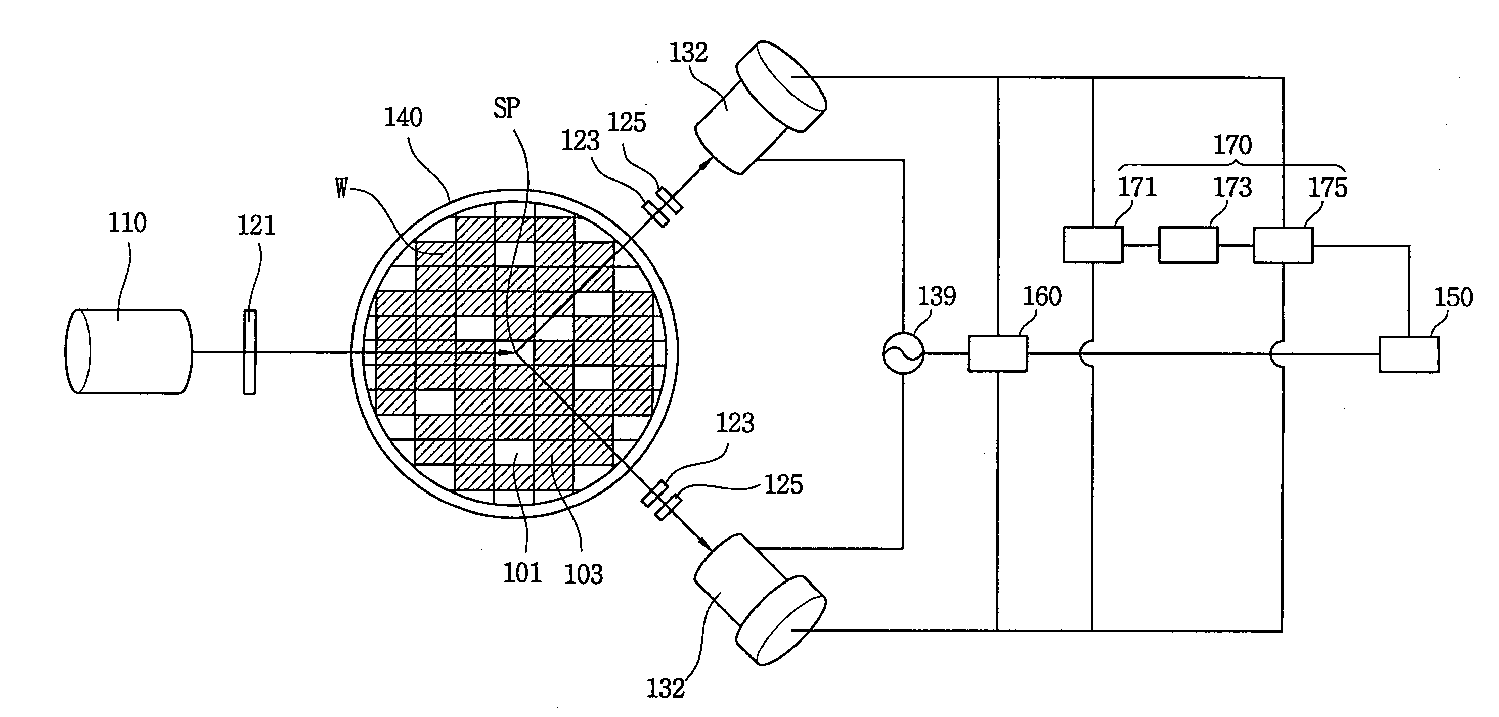
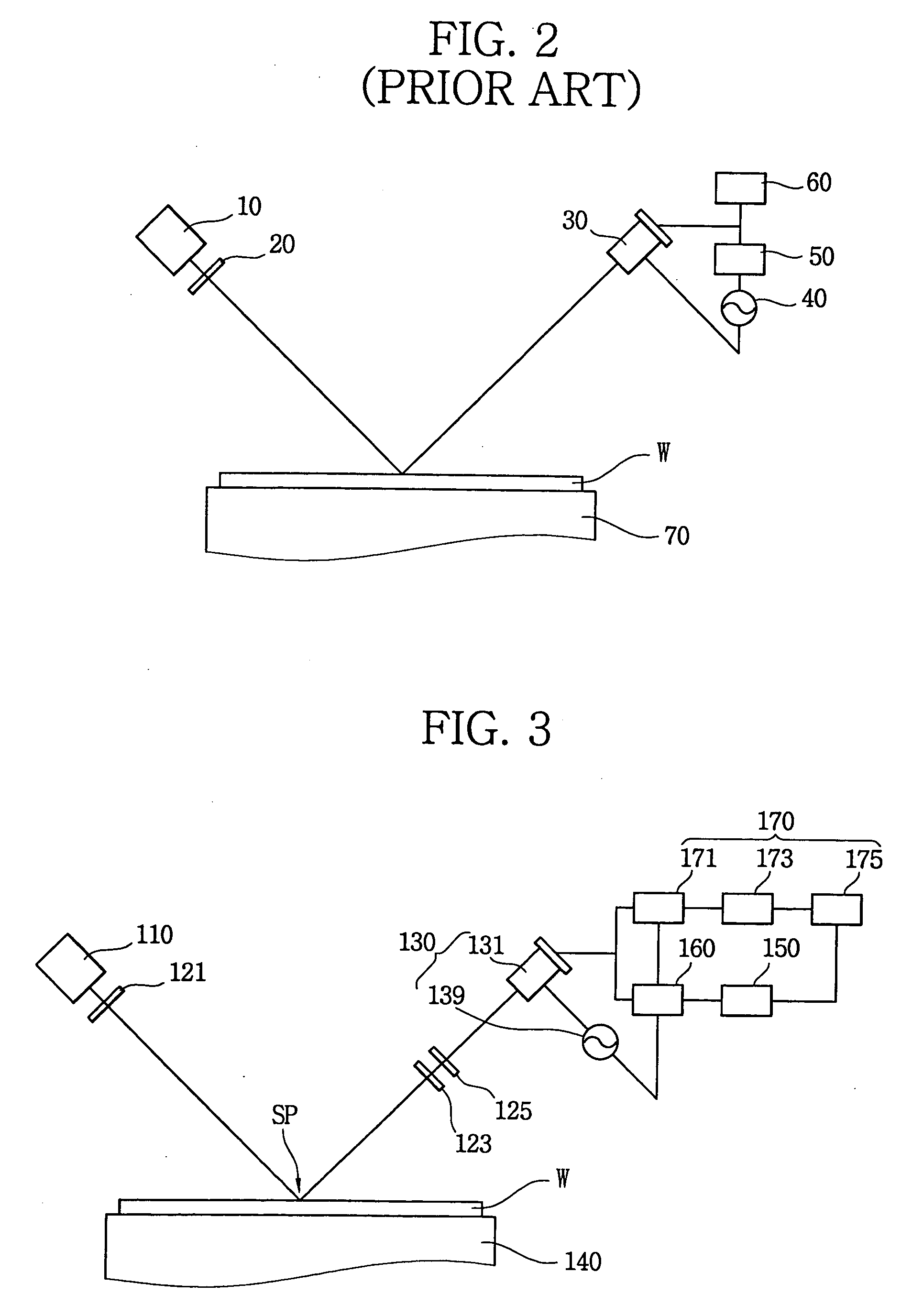
[0041] Referring to FIG. 3, an apparatus for inspecting a defect includes a stage 140 on which a wafer W is disposed. Here, a surface of the wafer W is divided into regions. An emitter 110 irradiates a light onto regions of the wafer W. A detector 130 collects light reflected from the wafer W. The detector 130 also amplifies the collected light by a pre...


PUM

PropertyMeasurementUnit
angleaaaaaaaaaa
angleaaaaaaaaaa
angleaaaaaaaaaa

Abstract

In a method for inspecting a defect in accordance with one aspect of the present invention, an object is divided into a plurality of regions. Reflectivity of each of the plurality of regions is obtained. Amplification ratio for each region is determined using the reflectivity. A light is irradiated onto the regions. A light reflected from a first region is amplified by a first amplification ratio that is determined for the first region. Moving the irradiated light from the first region to a second region is detected. A light reflected from the second region is amplified by a second amplification ratio that is determined for the second region. The amplified lights from the first region and the second region are analyzed to determine an existence of a defect on the object.

Description

CROSS REFERENCE TO RELATED APPLICATION [0001] This application claims priority under 35 USC § 119 to Korean Patent Application No. 2003-53537, filed on Aug. 1, 2003, the content of which is herein incorporated by reference in its entirety for all purposes. BACKGROUND OF THE INVENTION [0002] 1. Field of the Invention [0003] The present invention relates to a method and an apparatus for inspecting. More particularly, the present invention relates to a method and an apparatus for conducting a rapid and accurate inspection of a defect, for example, a particle and / or a scratch that exists on a semiconductor substrate. [0004] 2. Description of the Related Arts [0005] To process massive data in a short time, a semiconductor device has been highly integrated. To manufacture the highly-integrated semiconductor device, a method of precisely depositing a thin film pattern on a semiconductor substrate is very important. Accordingly, an inspection process for determining a failure of the thin fi...

Claims


Application Information

Patent Timeline
Patent Type & Authority Applications(United States)
IPC IPC(8): H01L21/66G01N21/00G01N21/55G01N21/95
CPCG01N21/9501G01N21/55H01L22/00
Inventor KIM, JOUNG-SOOYANG, YU-SINKIM, MOON-KYUNGCHON, SANG-MUNCHOI, SUN-YONGJUN, CHUNG-SAM
Owner SAMSUNG ELECTRONICS CO LTD
Why Eureka
Try Eureka