Method for manufacturing semiconductor device

a semiconductor and manufacturing technology, applied in the direction of semiconductor devices, basic electric elements, electrical equipment, etc., can solve the problems of complicated steps of the whole process, inefficient filling of contact holes, and complicated steps of the process, so as to reduce the number of ion implant process steps, reduce the aspect ratio of contact holes, and reduce the number of process steps

Inactive Publication Date: 2005-05-05
STMICROELECTRONICS SRL +1
View PDF3 Cites 10 Cited by
  • Summary
  • Abstract
  • Description
  • Claims
  • Application Information

AI Technical Summary

Benefits of technology

[0014] One object of the present invention is to efficiently fill a contact hole by decreasing an aspect ratio of the contact hole.
[0015] Another object of the present invention is to prevent process failures from occurring in a process for forming metal lines due to a plurality of ion implant processes for increasing an impurity concentration which may be reduced in an impurity region after the process for forming the contact hole, by decreasing a number of the ion implant processes.
[0016] Yet another object of the present invention is to reduce steps of a process for forming multi-layer metal lines.

Problems solved by technology

Therefore, an aspect ratio of the contact hole increases, and thus the contact hole is not efficiently filled.
Accordingly, steps of the whole process are complicated.
Third, the first and second contact plugs and the first metal lines use different metal materials, to complicate the steps of the process.

Method used


Image

  • Method for manufacturing semiconductor device
  • Method for manufacturing semiconductor device
  • Method for manufacturing semiconductor device

Examples


Embodiment Construction

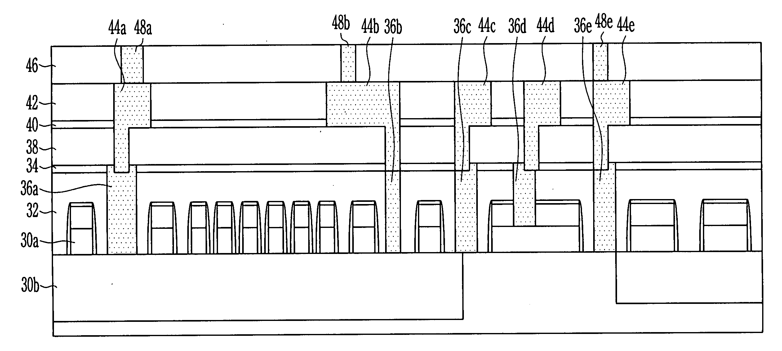
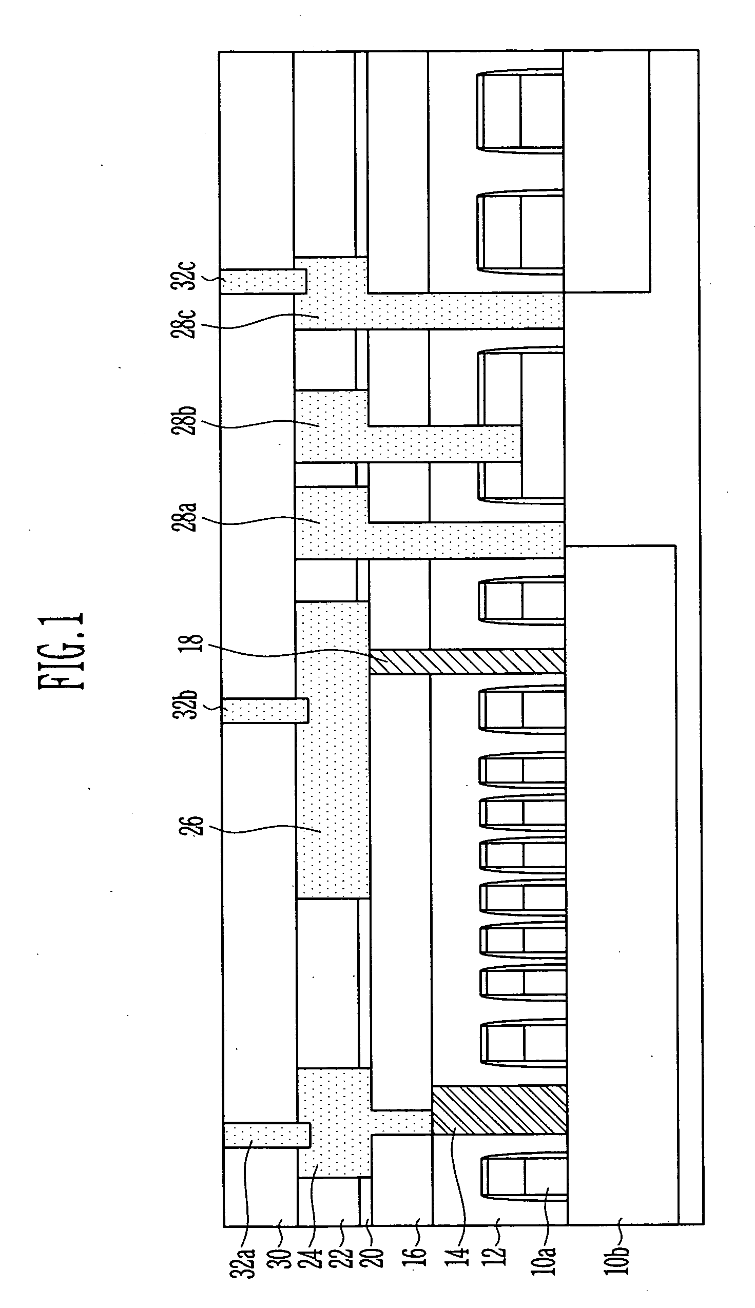
[0021] A method for manufacturing a semiconductor device in accordance with a preferred embodiment of the present invention will now be described in detail with reference to the accompanying drawings. In the drawings, a thickness of a film is exaggerated to emphasize clear and accurate explanations. Wherever possible, the same reference numerals will be used throughout the drawings and the description to refer to the same or like parts. In addition, in the case that it is described that one film is disposed on or contacts another film or a semiconductor substrate, one film can directly contact another film or the semiconductor substrate, or the third film can be positioned between them.

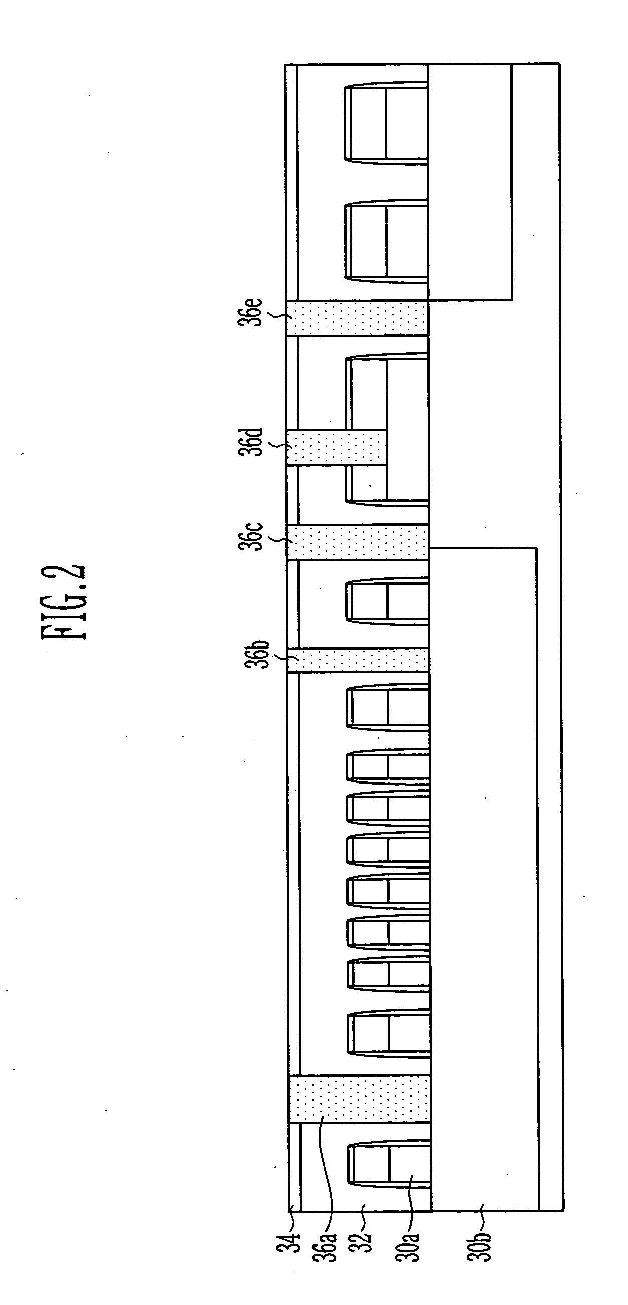
[0022] FIGS. 2 to 4 are cross-sectional diagrams illustrating sequential steps of a method for forming metal lines in a semiconductor device in accordance with a preferred embodiment of the present invention.

[0023] As illustrated in FIG. 2, an HDP oxide film 32 which is a first interlayer insulation...


PUM


Abstract

The present invention discloses a method for manufacturing a semiconductor device, comprising the steps of: providing a semiconductor substrate on which cell strings are formed and in which a plurality of conductive regions are formed; sequentially forming a first interlayer insulation film and a first etch barrier film on the semiconductor substrate; forming a plurality of contact holes by exposing the plurality of conductive regions formed in the semiconductor substrate, wherein an impurity concentration of the conductive regions is reduced due to the process for forming the contact holes; filling a metal material in the contact holes and forming a plurality of contact plugs; sequentially forming a second interlayer insulation film, a second etch barrier film and a third interlayer insulation film over a resulting structure including the contact plugs; forming a plurality of metal line patterns, wherein the metal line patterns pass through the third interlayer insulation film, the second etch barrier film and the second interlayer insulation film and contact to the contact plugs; forming a fourth interlayer insulation film over a resulting structure including the plurality of metal line patterns; forming a plurality of metal line contact holes by patterning the fourth interlayer insulation film; and forming a plurality of metal line contact plugs in the plurality of metal line contact holes by filling a metal material in the metal line contact holes.

Description

BACKGROUND [0001] 1. Field of the Invention [0002] The present invention relates to a method for manufacturing a semiconductor device, and more particularly to, a method for forming metal lines in a NAND flash memory device. [0003] 2. Discussion of Related Art [0004]FIG. 1 is a cross-sectional diagram illustrating a conventional metal line structure of a NAND flash memory device. A conventional method for forming metal lines will now be explained with reference to FIG. 1. [0005] Referring to FIG. 1, a first contact plug 14 exposing a conductive region in a predetermined region of a semiconductor substrate 10b including cell strings 10a is formed by patterning a first interlayer insulation film 12 on the whole surface of the semiconductor substrate 10b. [0006] A second contact plug 18 exposing a conductive region except the conductive region in which the first contact plug 14 has been formed is formed by patterning a first interlayer insulation film 12 and a second interlayer insulat...

Claims


Application Information

Patent Timeline
Patent Type & Authority Applications(United States)
IPC IPC(8): H01L21/28H01L21/3205H01L27/115H01L21/44H01L21/4763H01L21/768H01L21/8239H01L27/105
CPCH01L21/76838H01L27/1052H01L27/105H10B99/00H10B69/00
Inventor JEONG, CHEOL MOKIM, TAE KYUNG
Owner STMICROELECTRONICS SRL
Why Eureka
Try Eureka