Semiconductor device and method for fabricating the same

a semiconductor device and semiconductor technology, applied in the direction of semiconductor devices, semiconductor/solid-state device details, electrical equipment, etc., can solve the problems of insufficiently preventing moisture or the like from entering the region surrounded by the seal ring from the outside, affecting the and affecting the performance of the device. , to achieve the effect of preventing chipping, breaking, and preventing degradation of the moisture resistance and reliability of the semiconductor devi

Active Publication Date: 2005-05-12
PANASONIC CORP
View PDF17 Cites 160 Cited by
  • Summary
  • Abstract
  • Description
  • Claims
  • Application Information

AI Technical Summary

Benefits of technology

[0037] As described above, according to the present invention, in a semiconductor device including a chip region and a seal ring structure provided in a peripheral part of the chip region and surrounding an element, interconnect layers and others in the chip region, a seal ring structure including a small number of “junctions” between its components is provided, a protection film has an opening on the seal ring structure, and a cap layer is formed in the opening. This seal ring structure may partially include branches (e.g., at least two conductors serving as bridges in part of the seal ring structure) or may include two or more seal rings surrounding the chip region (e.g., a first seal ring formed in a peripheral part of the chip region and at least one seal ring surrounding the first seal ring.) With the foregoing features of the present invention, it is possible to prevent chipping, breaking and the like caused by dicing a wafer into chips (semiconductor devices) from reaching chip regions. Accordingly, it is also possible to prevent degradation of the moisture resistance and reliability of the semiconductor devices.

Problems solved by technology

However, the conventional semiconductor device has the problem that the passivation film peels off by impact caused during dicing of a wafer or the problem that the impact propagates through the passivation film to reach the inside of the chip region.
If the passivation film has an opening on the seal ring and the upper part of the seal ring is exposed in the opening as in the semiconductor device disclosed in reference 1, it is impossible to sufficiently prevent moisture or the like from entering a region surrounded by the seal ring from the outside.
However, the low-κ interlayer dielectric films generally have low mechanical strength, so that the low-κ interlayer dielectric films exhibit insufficient durability against stress occurring during dicing, as compared to interlayer dielectric films made of conventional materials.
Therefore, the low-κ interlayer dielectric films are susceptible to damage during dicing.
Accordingly, even if a seal ring is formed by alternately using masks for vias and masks for interconnects in a peripheral part of a chip region in a semiconductor device using such low-κ interlayer dielectric films as in the conventional device, damage during dicing is not sufficiently prevented.
As a result, such junctions (or portions where components are not connected) act as paths through which impact propagates, so that it is impossible to prevent cracks or the like occurring during dicing from propagating into chip regions.

Method used


Image

  • Semiconductor device and method for fabricating the same
  • Semiconductor device and method for fabricating the same
  • Semiconductor device and method for fabricating the same

Examples


embodiment 1

[0063] Hereinafter, a semiconductor device and a method for fabricating the device according to a first embodiment of the present invention will be described with reference to drawings.

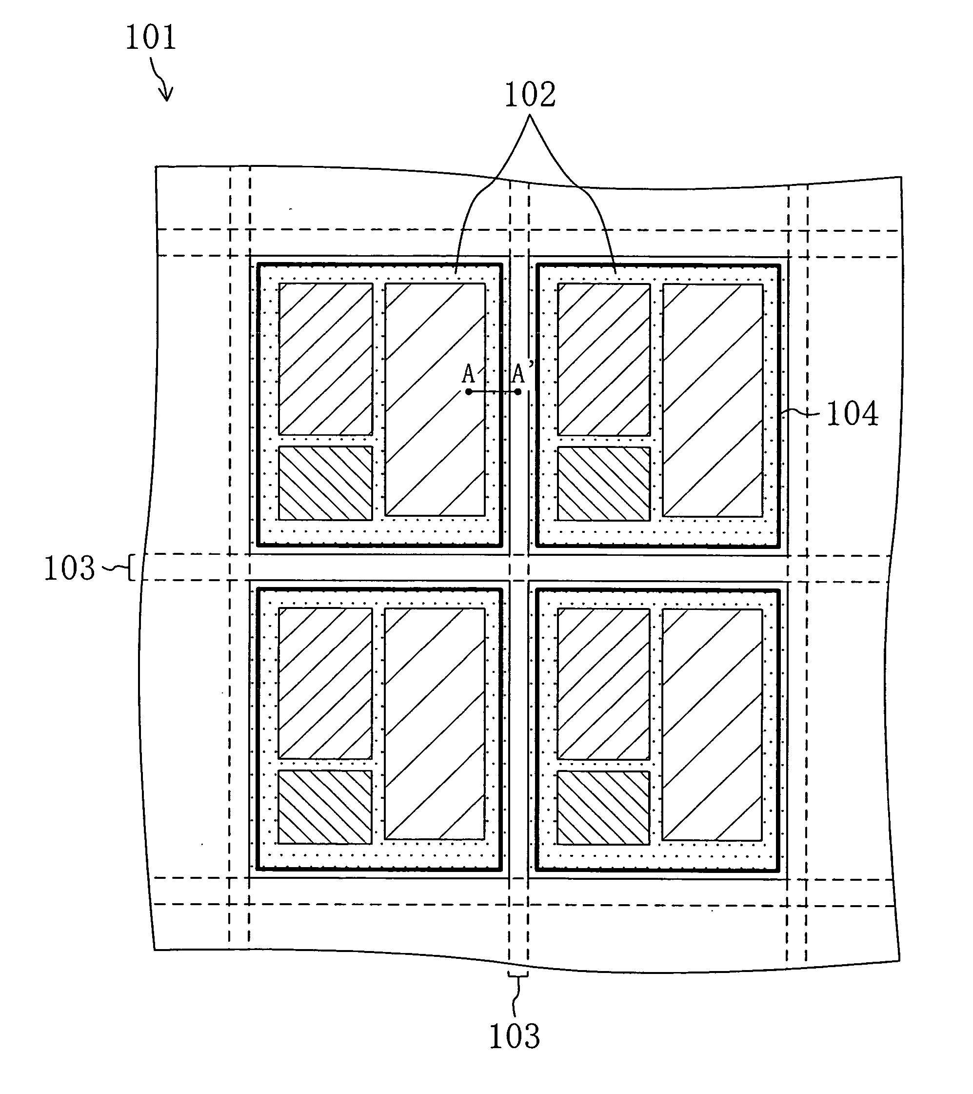
[0064]FIG. 1 is a plan view showing part of a wafer on which the semiconductor device of the first embodiment (i.e., a semiconductor device in which one seal ring surrounds a chip region) is provided.

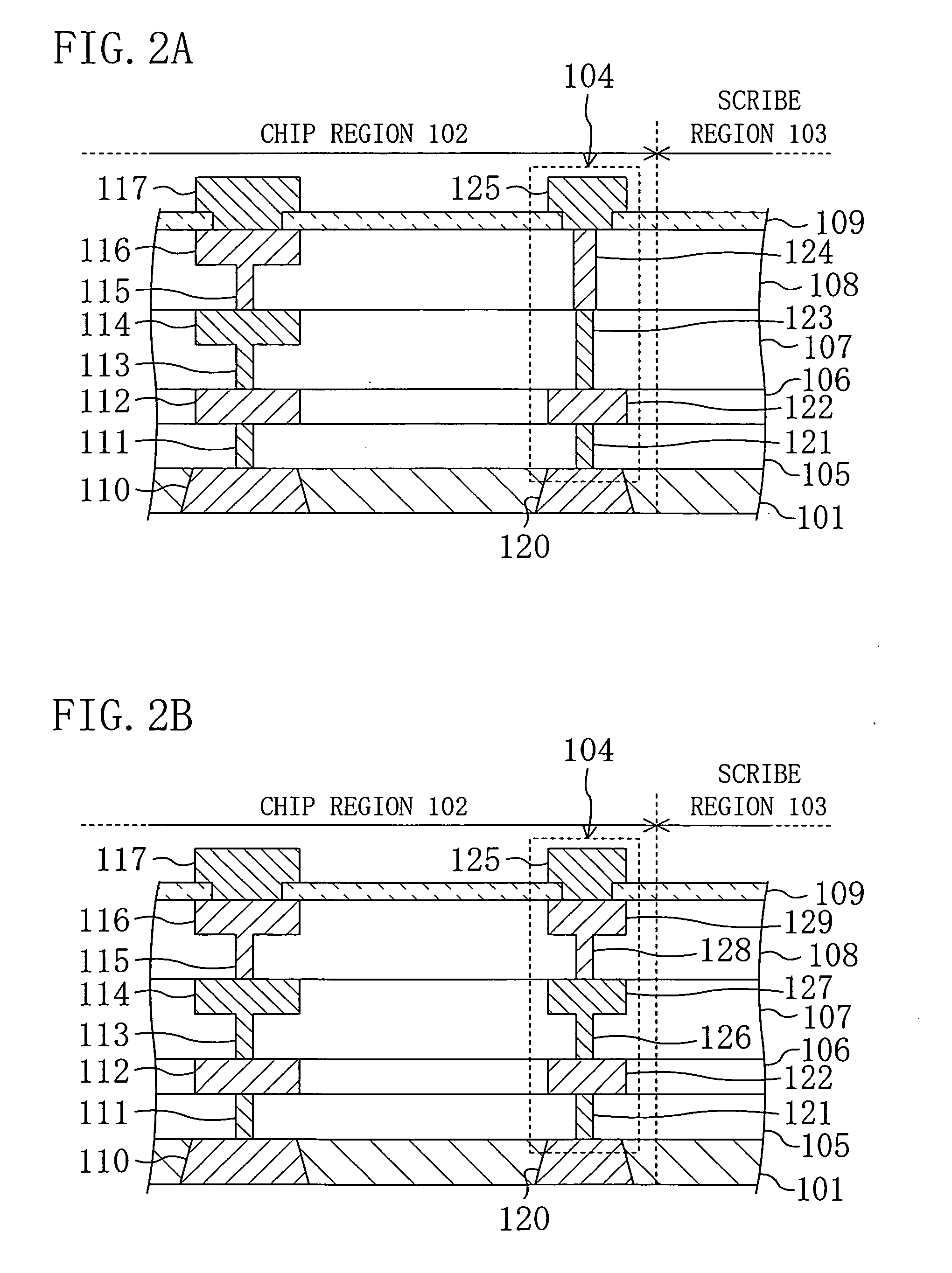
[0065] As shown in FIG. 1, on a wafer 101 to be a semiconductor substrate, which is typically a silicon substrate, for example, a plurality of chip regions 102 to be semiconductor devices are provided. In each of the chip regions 102, an integrated circuit (IC) made of a plurality of elements and provided with a given function is formed. The chip regions 102 are defined by a scribe region 103 having a lattice pattern.

[0066] A semiconductor device (i.e., a semiconductor chip) includes: a chip region 102 on which an IC made of a plurality of elements and provided with a given function is formed; and a se...

embodiment 2

[0128] Hereinafter, a semiconductor device and a method for fabricating the device according to a second embodiment of the present invention will be described with reference to drawings.

[0129]FIG. 7 is a plan view showing part of a wafer on which a semiconductor device of the second embodiment (i.e., a semiconductor device in which a chip region is surrounded by two seal rings) is provided. Hereinafter, a seal ring structure including two or more seal rings surrounding a chip region will be also referred to as a multi-seal ring structure.

[0130] As shown in FIG. 7, on a wafer 201 to be a semiconductor substrate, typically a silicon substrate, for example, a plurality of chip regions 202 to be semiconductor devices, are provided. In each of the chip regions 202, an IC made of a plurality of elements and provided with a given function is formed. The chip regions 202 are defined by a scribe region 203 having a lattice pattern.

[0131] A semiconductor device (i.e., a semiconductor chip)...

modified example 1 of embodiment 2

[0181] Hereinafter, a semiconductor device and a method for fabricating the device according to a first modified example of the second embodiment will be described with reference to drawings.

[0182]FIG. 12A is a cross-sectional view (a view showing the cross-sectional structure taken along the line B-B′ in FIG. 7) of a semiconductor device according to this modified example.

[0183] The seal ring structure of this modified example shown in FIG. 12A is different from that of the second embodiment shown in FIG. 8A in that the cap layer (first cap layer) 225a is not provided at the top of the inner seal ring (first seal ring) 204a. In other words, the passivation film 209 has no opening on the first seal ring 204a.

[0184] Specifically, as shown in FIG. 12A, the semiconductor device of this modified example has a double seal ring structure as in the second embodiment. An outer second seal ring 204b in this structure includes a cap layer (second cap layer) 225b at its top as in the seal r...


PUM


Abstract

A seal ring structure is formed through a multilayer structure of a plurality of dielectric films in a peripheral part of a chip region to surround the chip region. A dual damascene interconnect in which an interconnect and a plug connected to the interconnect are integrated is formed in at least one of the dielectric films in the chip region. Part of the seal ring structure formed in the dielectric film in which the dual damascene interconnect is formed is continuous. A protection film formed on the multilayer structure has an opening on the seal ring. A cap layer connected to the seal ring is formed in the opening.

Description

CROSS-REFERENCE TO RELATED APPLICATION [0001] This application is related to Japanese Patent Application No. 2003-379754 filed on Nov. 10, 2003, whose priority is claimed under 35 USC §119, the disclosure of which is incorporated by reference in its entirety. BACKGROUND OF THE INVENTION [0002] The present invention relates to a semiconductor device having a seal ring structure surrounding a chip region and to a method for fabricating the device. [0003] A semiconductor device is generally fabricated by arranging a large number of integrated circuits (ICs) constituted by a plurality of elements and provided with given functions on a semiconductor wafer of, for example, silicon. [0004] A large number of chip regions arranged on a wafer are separated from each other by a scribe region (scribe line) having a lattice pattern. After the large number of chip regions have been formed on a wafer through a semiconductor fabrication process, the wafer is diced into chips along the scribe region...

Claims


Application Information

Patent Timeline
Patent Type & Authority Applications(United States)
IPC IPC(8): H01L23/00H01L23/522H01L23/58
CPCH01L23/522H01L23/564H01L23/585H01L2924/12044H01L2924/0002H01L23/562H01L2924/00H01L23/3171H01L23/3192H01L23/5226H01L23/528
Inventor TSUTSUE, MAKOTOUTSUMI, MASAKI
Owner PANASONIC CORP
Why Eureka
Try Eureka