Method for manufacturing semiconductor device

Active Publication Date: 2015-12-31
FUJI ELECTRIC CO LTD
View PDF12 Cites 7 Cited by
  • Summary
  • Abstract
  • Description
  • Claims
  • Application Information

AI Technical Summary

Benefits of technology

[0025]According to the method for manufacturing the semiconductor device of the invention, it is possible to easily peel the supporting substrate bonded to the wafer. In addition, according to the method

Problems solved by technology

However, the TAIKO process has a limitation in manufacturing an

Method used


Image

  • Method for manufacturing semiconductor device
  • Method for manufacturing semiconductor device
  • Method for manufacturing semiconductor device

Examples


embodiment 1

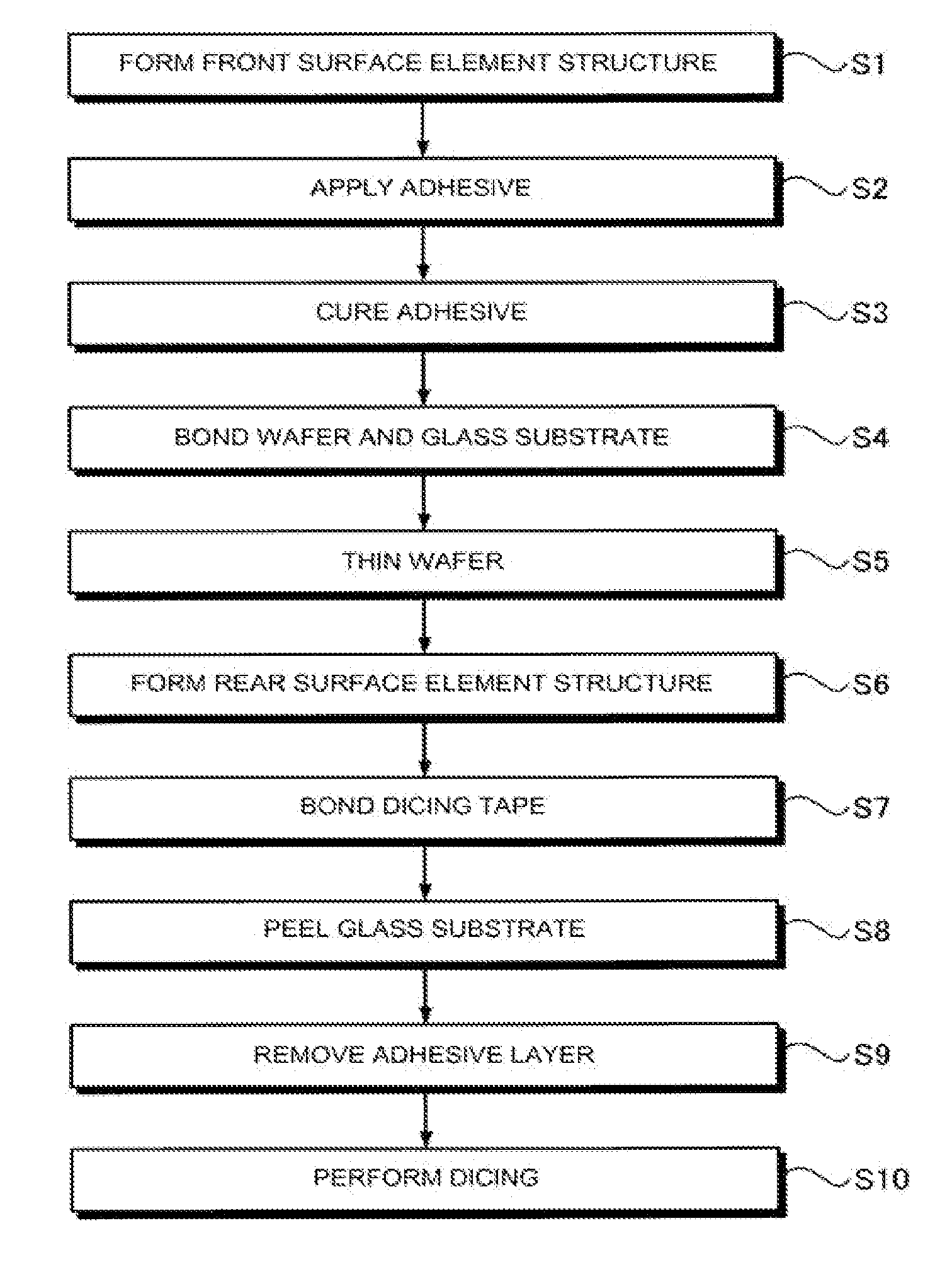
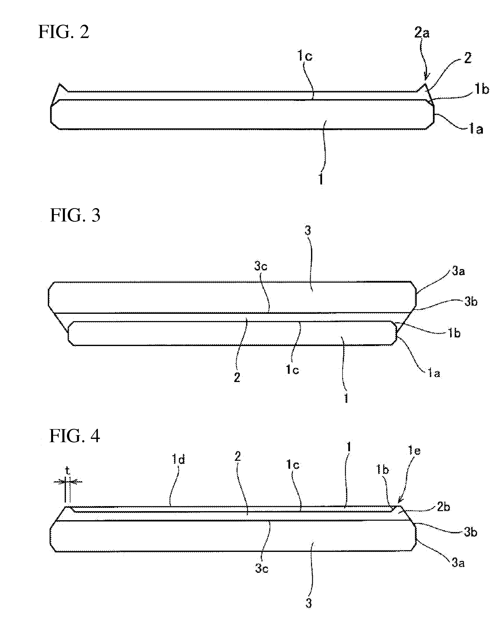
[0048]A method for manufacturing a semiconductor device according to Embodiment 1 will be described. FIG. 1 is a flowchart illustrating the outline of the method for manufacturing a semiconductor device according to Embodiment 1. FIGS. 2 to 5 are cross-sectional views illustrating states during manufacture in the flowchart illustrated in FIG. 1. First, processing is performed on a front surface of a general wafer 1 to form a front surface element structure (not illustrated) on a front surface (first main surface) 1c of the wafer 1 (Step S1). Then, an adhesive 2 is applied onto the entire front surface 1c of the wafer 1 by a coater (Step S2). In Step S2, for example, a spinning method which rotates the wafer 1 fixed to a stage at a high speed to spread the adhesive 2 applied onto the front surface 1c of the wafer 1 using centrifugal force is used.

[0049]The upper and lower ends (corners: hereinafter, referred to as chamfered portions) 1b of a side surface 1a of the wafer 1 are chamfer...

embodiment 2

[0064]Next, a method for manufacturing a semiconductor device according to Embodiment 2 will be described. FIG. 6 is a flowchart illustrating the outline of the method for manufacturing the semiconductor device according to Embodiment 2. FIGS. 7 to 9 are cross-sectional views illustrating states during manufacture in the flowchart illustrated in FIG. 6. The method for manufacturing the semiconductor device according to Embodiment 2 differs from the method for manufacturing the semiconductor device according to Embodiment 1 in that a process (Step S21) of removing an extra portion of an adhesive layer 22 is added between Step S5 and Step S6. That is, in Embodiment 2, when a wafer 1 and a glass substrate 3 are bonded to each other and a chamfered portion 3b and a side surface 3a of the glass substrate 3 are covered by a protruding portion in the outer circumference of an adhesive layer 22, the extra portion of the adhesive layer 22 is removed.

[0065]Specifically, first, similarly to Em...

embodiment 3

[0070]Next, a method for manufacturing a semiconductor device according to Embodiment 3 will be described. FIG. 11 is a flowchart illustrating the outline of the method for manufacturing the semiconductor device according to Embodiment 3. FIGS. 12 and 13 are cross-sectional views illustrating a state during manufacture in the flowchart illustrated in FIG. 11. The method for manufacturing the semiconductor device according to Embodiment 3 differs from the method for manufacturing the semiconductor device according to Embodiment 1 in that a process (Step S31) of removing an extra portion of an adhesive layer 32 is added between Step S6 and Step S7. That is, in Embodiment 3, similarly to Embodiment 2, when a wafer 1 and a glass substrate 3 are bonded to each other and a chamfered portion 3b and a side surface 3a of the glass substrate 3 are covered by a protruding portion in the outer circumference of an adhesive layer 32, the extra portion of the adhesive layer 32 is removed.

[0071]Spe...


PUM

PropertyMeasurementUnit
Thicknessaaaaaaaaaa
Areaaaaaaaaaaa

Abstract

A glass substrate is bonded to a front surface of a wafer on which a front surface element structure is formed, with an adhesive layer interposed therebetween. An adhesive layer is formed on the wafer to extend from the front surface of the wafer to a chamfered portion and a side surface of the wafer. The adhesive layer is formed on a first surface of the glass substrate and is not formed on a chamfered portion and a side surface of the glass substrate. After the rear surface of the wafer is ground, a rear surface element structure is formed on the ground rear surface. A laser beam is radiated to the glass substrate and the glass substrate is peeled from the adhesive layer. The adhesive layer is removed and the wafer is cut by dicing. In this way, a chip having a thin semiconductor device formed thereon is completed.

Description

TECHNICAL FIELD[0001]The present invention relates to a method for manufacturing a semiconductor device.BACKGROUND ART[0002]A thin semiconductor device which has a smaller thickness than the existing semiconductor device has been developed in order to improve the performance of a semiconductor device made of, for example, silicon (Si), silicon carbide (SiC), or gallium nitride (GaN). When the thin semiconductor device is manufactured, for example, a front surface element structure and a front surface electrode are formed on the front surface side of a wafer, the rear surface of the wafer is ground to a desired thickness (the wafer is thinned), and a rear surface element structure is formed on the ground rear surface of the wafer.[0003]In recent years, as a technique for reducing the thickness of the wafer, the following processes have been known: a TAIKO (registered trademark) process which leaves an outer circumferential portion of the wafer as a reinforcing portion (rib portion) a...

Claims


Application Information

Patent Timeline
IPC IPC(8): H01L21/683H01L21/304B32B38/00B32B37/12B32B37/18
CPCH01L21/6835B23K26/57H01L2221/68327H01L2221/6834H01L2221/68386H01L21/304B32B38/10B32B2315/08B32B38/0012B32B37/18B32B37/1284H01L2221/68377B32B2457/14B32B2038/0016H01L2221/68381B32B7/06B32B17/06H01L21/6836
Inventor NAKAJIMA, TSUNEHIRO
Owner FUJI ELECTRIC CO LTD
Why Eureka
Try Eureka