Silicon device on Si:C-OI and SGOI and method of manufacture

Active Publication Date: 2005-05-19
IBM CORP
View PDF99 Cites 72 Cited by
  • Summary
  • Abstract
  • Description
  • Claims
  • Application Information

AI Technical Summary

Benefits of technology

[0012] In a first aspect of the invention, a method of manufacturing a structure includes forming shallow trench isolation (STI) in a substrate and providing a first material and a second material on the substrate. The first material and the second material are mixed into the substrate by a thermal anneal process to form a first island and second isla

Problems solved by technology

However, the same stress component, either tensile stress or compressive stress, discriminatively affects the characteristics of an n-type device and a p-type device.
That is, because the type of stress which is beneficial for the performance of an nFET is generally disadvantageous for the performance of the pFET.
Unfortunately, the tensilely strained Si on relaxed SiGe can apply only biaxial tensile stress on the Si cap as used in stack form.
This level of Ge % is difficult to implement into processes and is not very manufacturable with major issues including surface roughness, process complexity, defect and yield control, to name but a few.
Given that a hi

Method used


Image

  • Silicon device on Si:C-OI and SGOI and method of manufacture
  • Silicon device on Si:C-OI and SGOI and method of manufacture
  • Silicon device on Si:C-OI and SGOI and method of manufacture

Examples


Embodiment Construction

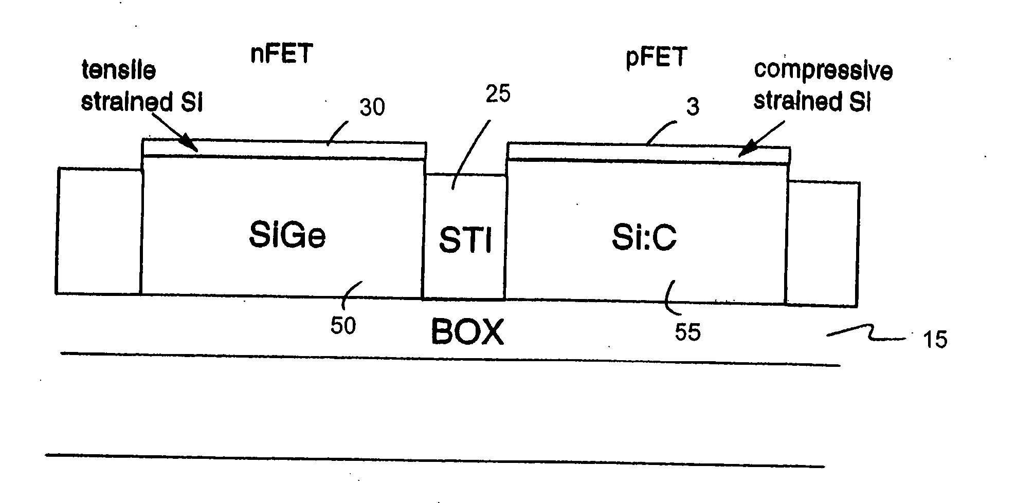
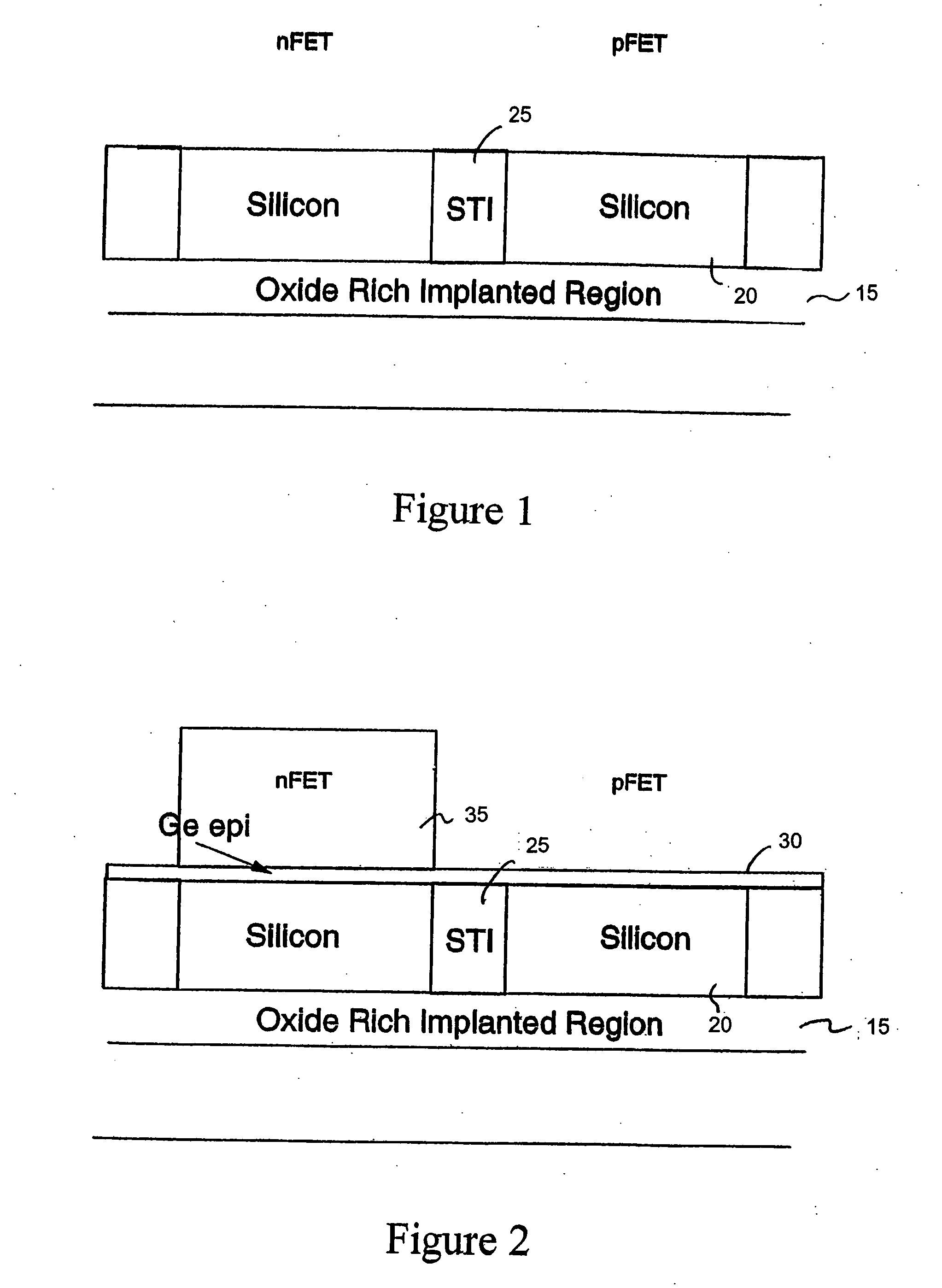
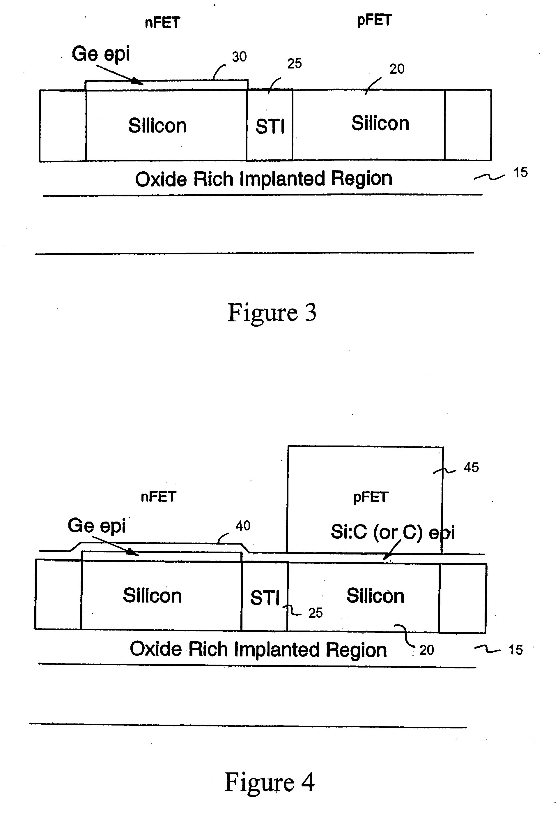
[0022] This invention is directed to a semiconductor device and method of manufacture which provides desired stresses in the nFET channel and the pFET channel of CMOS devices for improved device performance. In one approach, a SiGe island is obtained through thermally mixing deposited Ge material into an SOI thin film. Similarly, a Si:C island is obtained through thermally mixing deposited Si:C or C into the Si or SOI thin film. By using the method of the invention, the required Ge % is not large and thus does not cause defect issues. Also, relaxation of SiGe and / or Si:C islands in the channels of the pFET and nFET, respectively, can be achieved by the invention to thus provide improved performance as compared to blanket (SiGe or Si:C) substrates. This is because, in the implementations of the invention, a high temperature thermal mixing step, for example, is provided such that shallow trench isolation (STI) can relax and facilitate the relaxation of the SiGe and Si:C islands.

[0023...


PUM


Abstract

A semiconductor structure and method of manufacturing is provided. The method of manufacturing includes forming shallow trench isolation (STI) in a substrate and providing a first material and a second material on the substrate. The first material and the second material are mixed into the substrate by a thermal anneal process to form a first island and second island at an nFET region and a pFET region, respectively. A layer of different material is formed on the first island and the second island. The STI relaxes and facilitates the relaxation of the first island and the second island. The first material may be deposited or grown Ge material and the second material may deposited or grown Si:C or C. A strained Si layer is formed on at least one of the first island and the second island.

Description

BACKGROUND OF THE INVENTION [0001] 1. Field of the Invention [0002] The invention generally relates to a semiconductor device and method of manufacture and, more particularly, to a semiconductor device and method of manufacture which imposes tensile and compressive stresses in the device during device fabrication. [0003] 2. Background Description [0004] Mechanical stresses within a semiconductor device substrate can modulate device performance. That is, stresses within a semiconductor device are known to enhance semiconductor device characteristics. Thus, to improve the characteristics of a semiconductor device, tensile and / or compressive stresses are created in the channel of the n-type devices (e.g., nFETs) and / or p-type devices (e.g., pFETs). However, the same stress component, either tensile stress or compressive stress, discriminatively affects the characteristics of an n-type device and a p-type device. [0005] In order to maximize the performance of both nFETs and pFETs within...

Claims


Application Information

Patent Timeline
IPC IPC(8): H01L21/82H01L21/8238H01L21/84H01L27/12H01L29/24H01L29/808
CPCH01L21/8213H01L21/823807H01L21/84H01L27/1203H01L29/1054H01L29/1095H01L29/66651H01L29/7843H01L29/7846H01L29/8086H01L29/0649H01L29/1608H01L21/823412H01L29/7378H01L29/7849
Inventor CHIDAMBARRAO, DURESETIDOKUMACI, OMER H.GLUSCHENKOV, OLEG G.
Owner IBM CORP
Why Eureka
Try Eureka