Circuit device and manufacturing method thereof

a technology of circuit devices and manufacturing methods, applied in the direction of printed circuit manufacturing, printed circuit non-printed electric components association, basic electric elements, etc., can solve the problems of large parasitic capacitances arising locally, the depth of isolation trenches is non-uniform, and the current capacity of conductive patterns b>81/b> is reduced, so as to facilitate circuit pattern design considering parasitic capacitances, the effect of uniform width and suppression of variation in the depth of trench

Inactive Publication Date: 2005-05-19
SANYO ELECTRIC CO LTD
View PDF7 Cites 15 Cited by
  • Summary
  • Abstract
  • Description
  • Claims
  • Application Information

AI Technical Summary

Benefits of technology

[0023] According to the circuit device of the present invention, a space between the conductive patterns is fixed. Thus, values of parasitic capacitances arising between the conductive patterns and the sealing resin can be easily predicted. Therefore, designing of a circuit pattern considering the parasitic capacitances is facilitated.
[0024] According to the method for manufacturing a circuit device of the present invention, the isolation trench is formed to have a uniform width. Thus, the isolation trench formed by etching also has a uniform depth. Therefore, the conductive patterns can be equally spaced apart. Furthermore, by forming the isolation trench to have a certain width or more, a variation in depth of the trench can be suppressed and a high-quality circuit device can be manufactured. Since the depth of the isolation trench is made uniform, conductive patterns having a desired thickness can be formed.

Problems solved by technology

However, when a width of the isolation trench 87 is narrowed in order to allow the conductive patterns 81 to come close to each other, there was a problem that a depth of the isolation trench 87 becomes nonuniform.
Thus, there was a problem that a current capacity of the conductive patterns 81 is reduced.
Moreover, when a space between the conductive patterns 81 becomes nonuniform, there was a problem that large parasitic capacitances arose locally.
This complicated the circuit design.

Method used


Image

  • Circuit device and manufacturing method thereof
  • Circuit device and manufacturing method thereof
  • Circuit device and manufacturing method thereof

Examples


Embodiment Construction

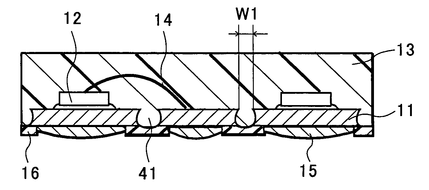
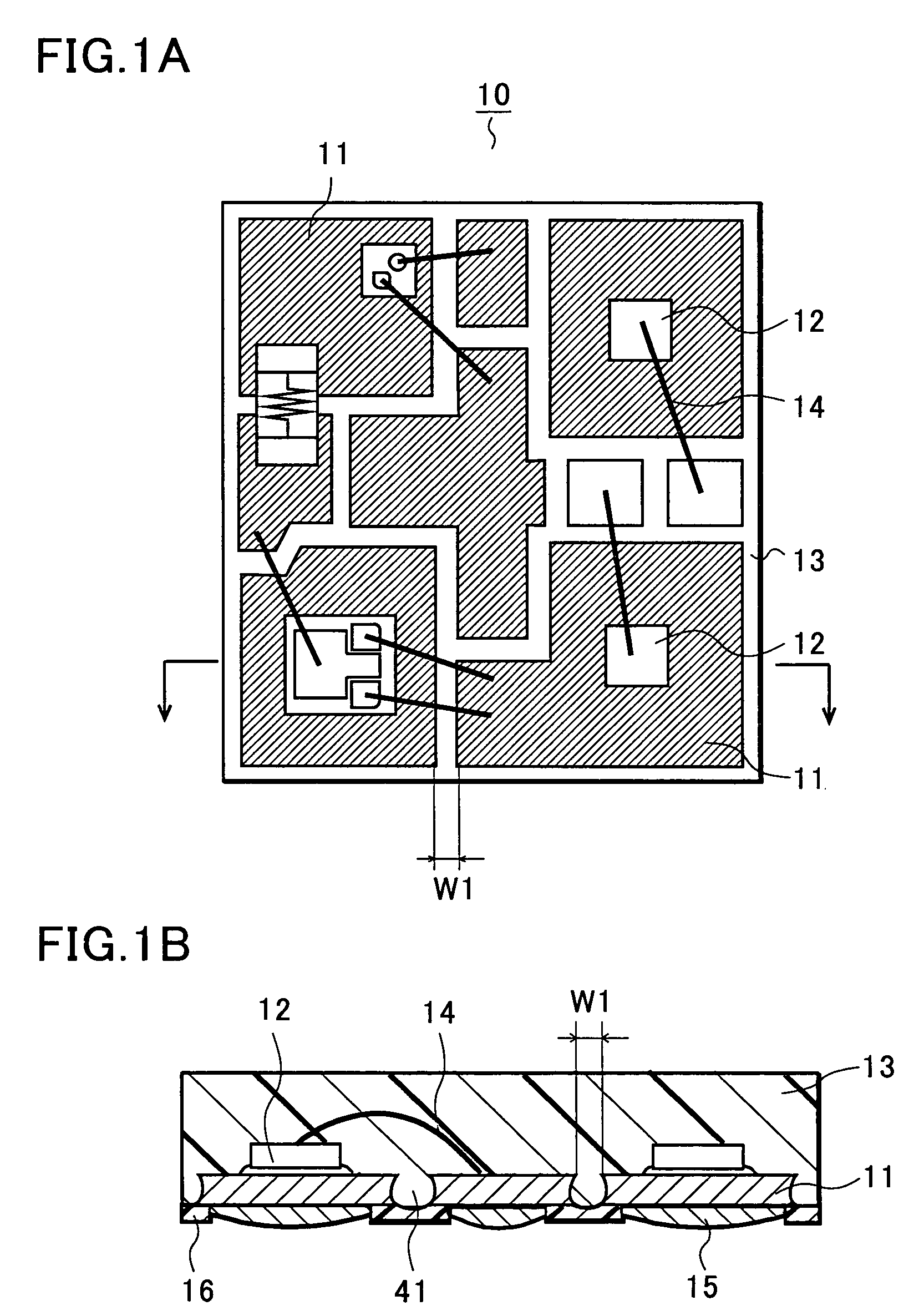
[0037] With reference to FIGS. 1A and 1B, description will be given of a configuration of a circuit device 10 of this embodiment. FIG. 1A is a plan view of a circuit device 10A and FIG. 1B is a cross-sectional view thereof.

[0038] With reference to FIG. 1A, the circuit device 10A of this embodiment includes: conductive patterns 11; circuit elements 12 electrically connected to the conductive patterns 11; and a sealing resin 13 covering the circuit elements 12 and the conductive patterns 11 while exposing back sides of the conductive patterns 11.

[0039] A material for the conductive patterns 11 is selected in consideration of adhesion, bonding and plating properties of a solder material. To be more specific, a conductive foil mainly made of Cu, a conductive foil mainly made of Al, a conductive foil made of alloy such as Fe—Ni, or the like is adopted as the material for the conductive patterns 11. Here, the conductive patterns 11 have a structure in which the patterns are buried in th...


PUM


Abstract

Provided is a circuit device having conductive patterns which are equally spaced apart and a manufacturing method thereof. A method for manufacturing a circuit device of the present invention includes the steps of: preparing a conductive foil; forming conductive patterns, which are included in a unit having at least regions for mounting circuit elements, by forming isolation trenches having a uniform width in the conductive foil; electrically connecting the conductive patterns to the circuit elements; sealing with a sealing resin so as to cover the circuit elements and to be filled in the isolation trenches; and removing the conductive foil in its thickness portions where no isolation trenches are provided.

Description

BACKGROUND OF THE INVENTION [0001] Priority is claimed to Japanese Patent Application Numbers JP2003-342082, filed on Sep. 30, 2003, and JP2004-251364, filed on Aug. 31, 2004, the disclosures of which are incorporated herein by reference in its entireties. [0002] 1. Field of the Invention [0003] The present invention relates to a circuit device and a manufacturing method thereof, more particularly to a circuit device having conductive patterns which are equally spaced apart and a manufacturing method thereof. [0004] 2. Description of the Related Art [0005] Conventionally, circuit devices set in electronic equipment have been required to be made smaller, thinner and lighter since the circuit devices are adopted in portable telephones, portable computers and the like. [0006] For example, as the circuit device, a semiconductor device will be described as an example. A wafer-scale CSP having the same size as a chip, which is called a CSP (chip size package), has been recently developed....

Claims


Application Information

Patent Timeline
Patent Type & Authority Applications(United States)
IPC IPC(8): H01L23/12H01L21/48H01L23/31H01L23/495H01L23/50H01L25/04H01L25/18H05K1/02H05K1/18H05K3/20
CPCH01L21/4832H01L2924/13055H01L23/49575H01L24/49H01L24/97H01L2224/48091H01L2224/48227H01L2224/48247H01L2224/48465H01L2224/49111H01L2224/49171H01L2224/73265H01L2224/97H01L2924/01004H01L2924/01005H01L2924/01006H01L2924/01013H01L2924/01015H01L2924/01028H01L2924/01029H01L2924/01033H01L2924/01059H01L2924/01074H01L2924/01078H01L2924/14H01L2924/19041H01L2924/19043H01L2924/30105H05K1/187H05K3/202H05K2203/0353H05K2203/0369H05K2203/1476H01L23/3107H01L2924/014H01L2924/01023H01L2224/32245H01L2224/32225H01L24/48H01L2924/00014H01L2224/85H01L2924/00H01L2924/00012H01L2224/451H01L2924/12042H01L24/45H01L24/73H01L2924/181H01L2224/05554H01L2224/0603H01L2924/19105H01L2924/00015H01L2224/05599H05K1/02
Inventor TAKAHASHI, KOUJI
Owner SANYO ELECTRIC CO LTD
Why Eureka
Try Eureka