Pixel structure for liquid crystal display

Active Publication Date: 2005-05-19
HANNSTAR DISPLAY CORPORATION
View PDF2 Cites 2 Cited by
  • Summary
  • Abstract
  • Description
  • Claims
  • Application Information

AI Technical Summary

Benefits of technology

[0007] In accordance with the foregoing description, it is the main object of the present invention to p

Problems solved by technology

Yet another problem is that even if the liquid crystal molecule 330 is transformed from splay orientation to bend orientation at the start of operation, the OCB cell m

Method used


Image

  • Pixel structure for liquid crystal display
  • Pixel structure for liquid crystal display
  • Pixel structure for liquid crystal display

Examples


first embodiment

THE FIRST EMBODIMENT

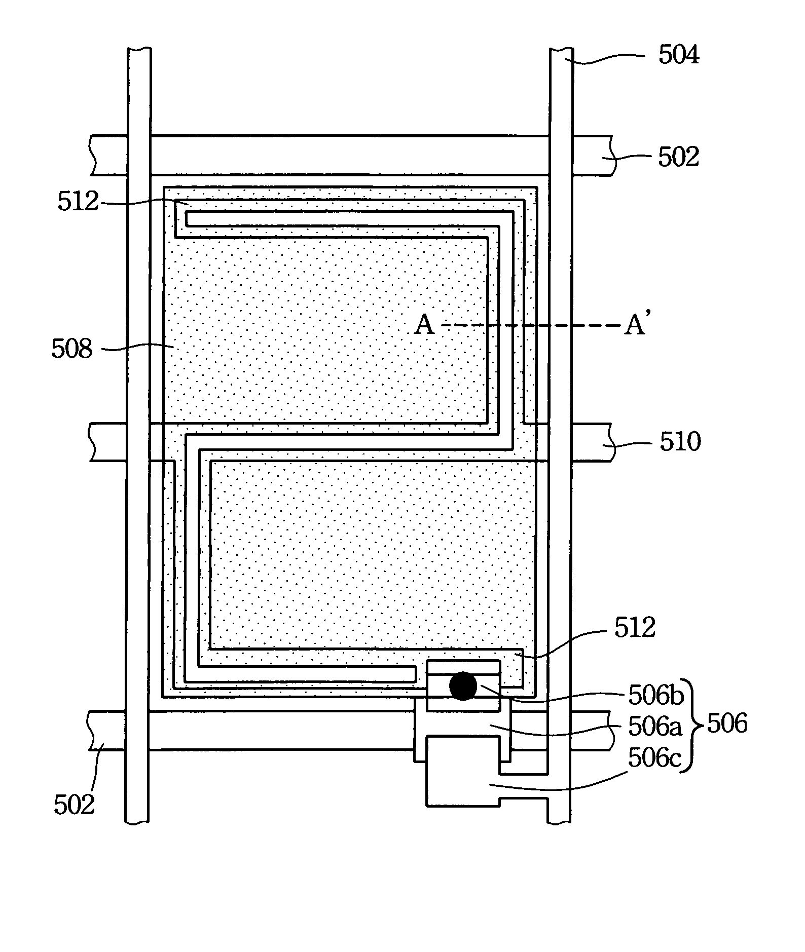
[0035]FIG. 2A shows a top view of the pixel region in accordance with the first embodiment of the present invention. The silicon island 506a of the switch transistor 506 is connected to the scan line 502. When the switch transistor 506 is selected, a scan signal is sent via the scan line 502 to turn the switch transistor 506 on. The video signal in the video data line 504 is transferred to the pixel electrode 508 through the switch transistor 506. The drain electrode 506b of the switch transistor 506 is connected to the pixel electrode 508. The source electrode 506c of the switch transistor 506 is connected to the video data line 504. A common electrode line 510 is used as the common electrode of the pixel electrode 508. An “S”-type metal electrode 512 is built around the pixel region. The metal electrode 512 is controlled by the common electrode line 510.

[0036] Typically, the source electrode 506c and the drain electrode 506b of the switch transistor 506 can re...

second embodiment

THE SECOND EMBODIMENT

[0056]FIG. 9A illustrates a schematic diagram of a pixel structure, in which a zigzag-shaped hole according to preferred embodiment is formed in the pixel electrode for exposing part of the common electrode line. The silicon island 550a of the switch transistor 550 is connected to the scan line 552. When the switch transistor 550 is selected, a scan signal is sent via the scan line 552 to turn the switch transistor 550 on. The video signal in the video data line 554 is transferred to the pixel electrode 556 through the switch transistor 550. The drain electrode 550b of the switch transistor 550 is connected to the pixel electrode 556. The source electrode 550c of the switch transistor 550 is connected to the video data line 554. When operating the liquid crystal display, a voltage is applied to a common electrode 558. Cooperating with the alignment direction of the liquid crystal molecules as indicated by the arrow 560, a continuous zigzag-shaped hole 562 in the...


PUM


Abstract

In accordance with the present invention, a mteal electrode or a common electrode line (both called as Vbias electrode) is built in the pixel region. Holes passing through the pixel electrode are formed in the positions corresponding to the mteal electrode or common electrode line (both called as Vbias electrode) so as to reduce the crosswise electrical field. The liquid crystal molecule in the whole pixel region is in a splay state.

Description

CROSS-REFERENCE TO RELATED APPLICATIONS [0001] This application is a continuation-in-part of U.S. application Ser. No. 10 / 936,752, filed on Sep. 9, 2004, and also a continuation-in-part of U.S. application Ser. No. 10 / 672,906, filed on Sep. 25, 2003, hereby incorporated by reference as it fully set forth herein.FIELD OF THE INVENTION [0002] The present invention relates to a pixel structure for a liquid crystal display and more particularly to a high-speed response pixel structure for a liquid crystal display. BACKGROUND OF THE INVENTION [0003] In recent years, studies on an OCB cell that is to be used as a liquid crystal cell instead of a TN cell have been made. An OCB cell is in a splay orientation state when no bias voltage is applied thereto, and exhibits a bend orientation state when a given high voltage is applied thereto. And in the bend orientation state, top and bottom liquid crystal molecules are always oriented symmetrically, thus compensates for the birefringence of liqu...

Claims


Application Information

Patent Timeline
IPC IPC(8): G02F1/133G02F1/1343G02F1/136G02F1/1368G02F1/139G09G3/20G09G3/36
CPCG02F1/1395G02F2001/134345G09G2310/06G09G3/3648G02F2201/121G02F1/134345
Inventor WU, ZHAO-HUISHIH, PO-SHENGYANG, KEI-HSIUNG
Owner HANNSTAR DISPLAY CORPORATION
Why Eureka
Try Eureka