Compact optical transceivers for host bus adapters

a technology of optical transceivers and host bus adapters, applied in the field of optical transceivers, can solve the problems of inability to integrate conventional optical transceivers into very small spaces, inability to meet the needs of such devices, and the body of conventional optical transceivers is still too wide and/or tall to fit within a typical pcmcia laptop envelope, etc., to achieve the effect of shortening the transceiver, reducing the space of the board, and reducing the size of the board

Inactive Publication Date: 2005-05-19
II VI DELAWARE INC
View PDF4 Cites 77 Cited by
  • Summary
  • Abstract
  • Description
  • Claims
  • Application Information

AI Technical Summary

Benefits of technology

[0020] As a result of the orientation of the transceiver substrate, the optical transceiver occupies relatively less board space than conventional transceivers, thus freeing board space for the inclusion of additional components and circuitry. Thus, the orientation of the transceiver substrate enables implementation of enhancements to the functionality of the device to which the optical transceiver is mounted. Moreover, the functionality of the optical transceiver itself is not compromised, since components and circuitry can be mounted to both sides of the vertically oriented transceiver substrate.
[0021] Additionally, the orientation of the transceiver substrate allows for production of relatively shorter transceivers that can be readily integrated within various devices, thus foreclosing the need for problematic external connections. These and other aspects of the present invention will become more fully apparent from the following description and appended claims, or may be learned by the practice of the invention as set forth hereinafter.

Problems solved by technology

In these, and other, applications however, conventional optical transceivers are typically not well suited for integration within such devices.
More specifically, the number of components within the transceiver, as well as the orientation and the size of SFF or SFP optical transceivers, makes it difficult, if not impossible, to integrate conventional optical transceivers into very small spaces, such as within a pluggable card for use in a laptop computer or hand held device.
For example, despite their relatively compact nature, conventional SFF, SFP, and XFP optical transceiver bodies are still too wide and / or tall to fit within a typical PCMCIA laptop envelope.
A related problem concerns the connections of the optical transceiver.
In particular, use of the optical transceiver as an external, rather than internal, component necessitates the use of additional connectors and connections, which increase both the overall cost associated with the system as well as the complexity of the system.
As well, optical transceivers employed in an external, rather than integrated, configuration are more prone to rough handling and damage than an integrated component.
Furthermore, even if the conventional optical transceiver could fit within such an envelope, the length of the conventional optical transceiver SFF, SFP, or XFP optical transceiver is such that the transceiver substrate takes up an inordinate amount of board space on the HBA or other component to which the optical transceiver is attached.
This problem is of particular concern in light of the concurrent demands for increases in functionality and decreases in component size.
These, and other, considerations make conventional optical transceivers less than ideal for integration within computer systems.
Unfortunately, typical manufacturing standards and optical transceivers have not effectively addressed these problems.
This is likely due in part to the fact that typical manufacturing constraints require, among other things, a minimum number of active and passive circuitry components to be present on a transceiver substrate.
Thus, a designer or manufacturer may have somewhat limited latitude in terms of the type and number of components to be included in an optical transceiver.
Other constraints along similar lines relate to engineering limitations, such that miniaturization of transceiver components becomes ever more complicated as components and mounting surfaces become smaller.
Moreover, increased manufacturing and engineering difficulty also translate into higher costs.

Method used


Image

  • Compact optical transceivers for host bus adapters
  • Compact optical transceivers for host bus adapters
  • Compact optical transceivers for host bus adapters

Examples


Embodiment Construction

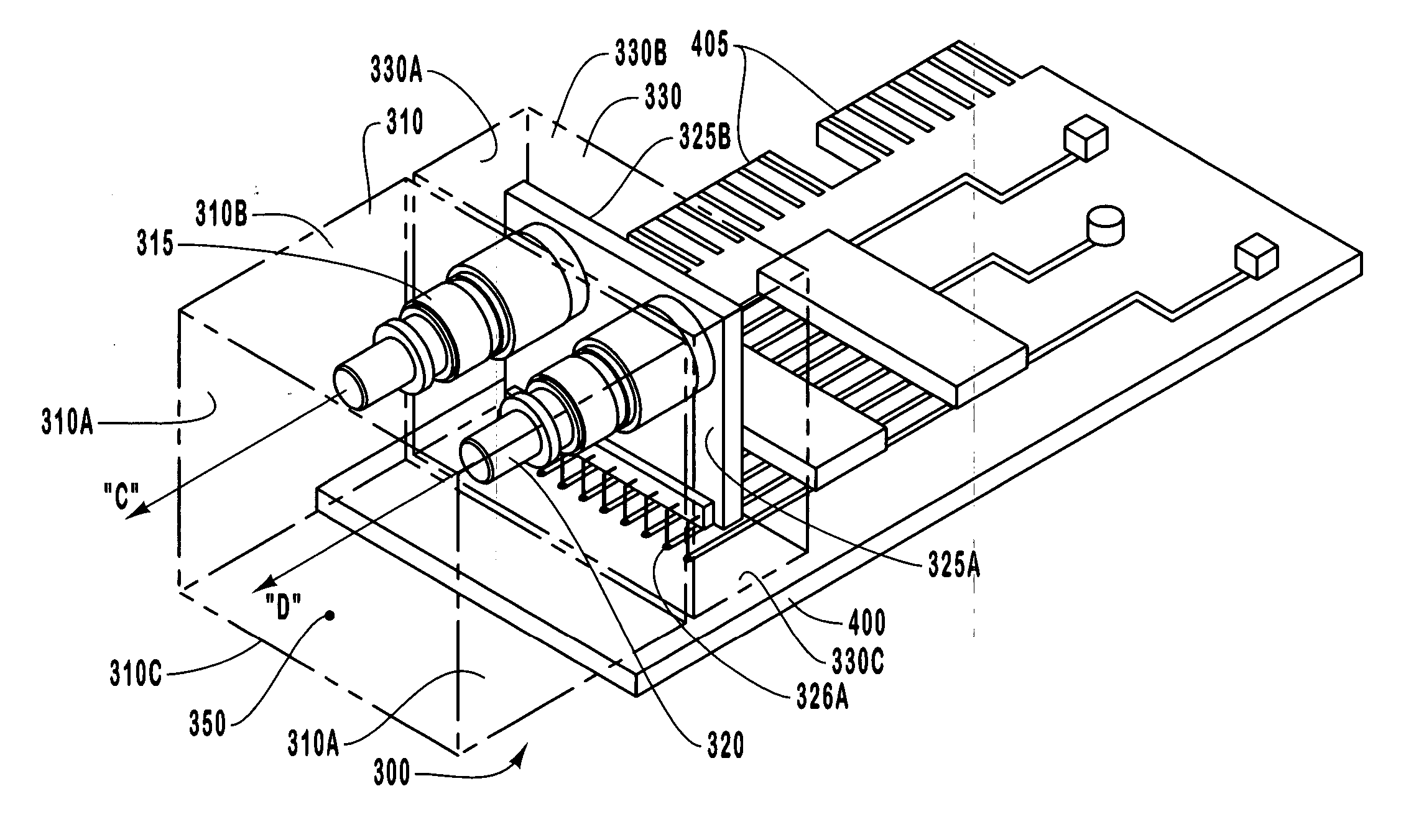
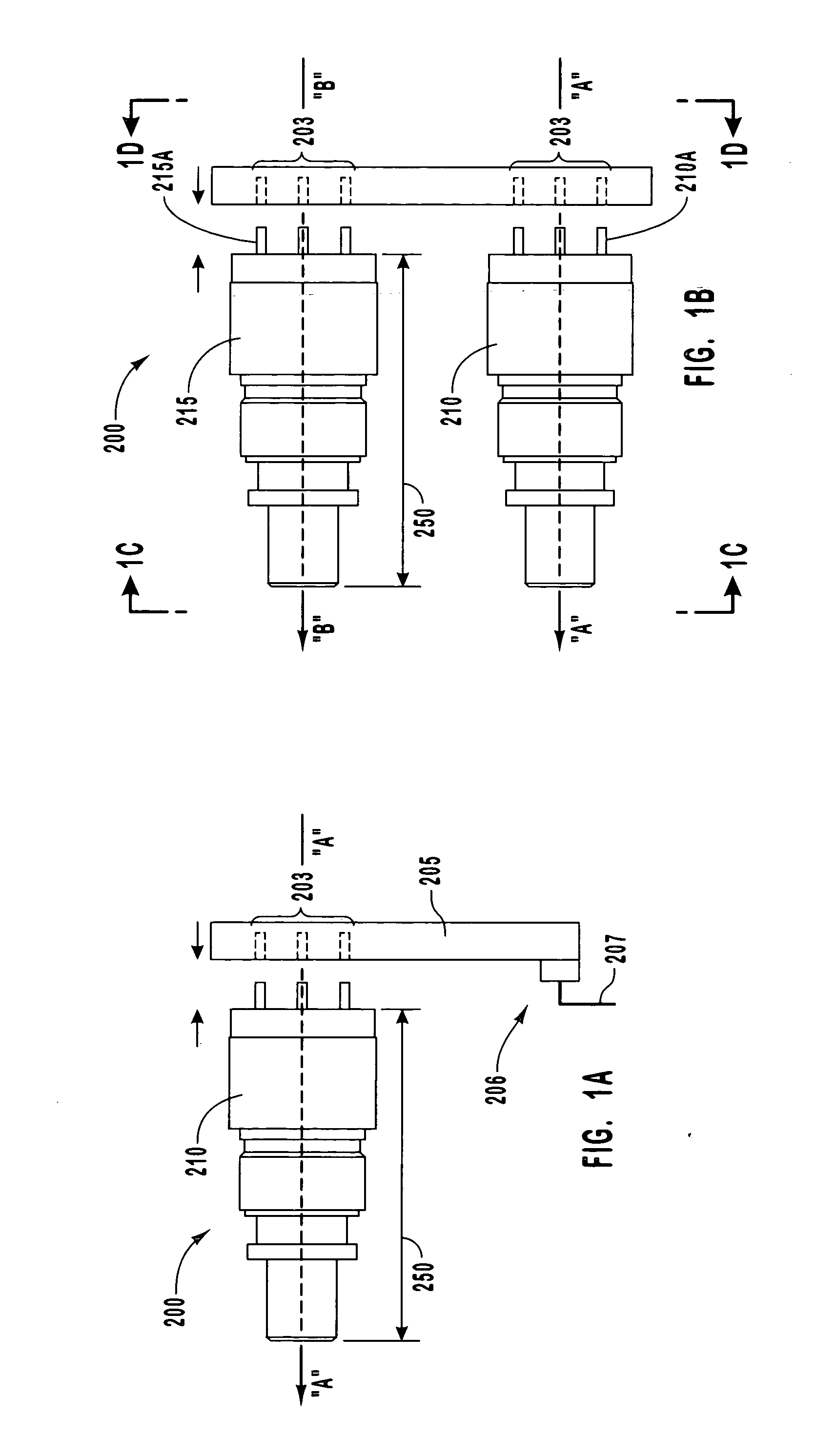
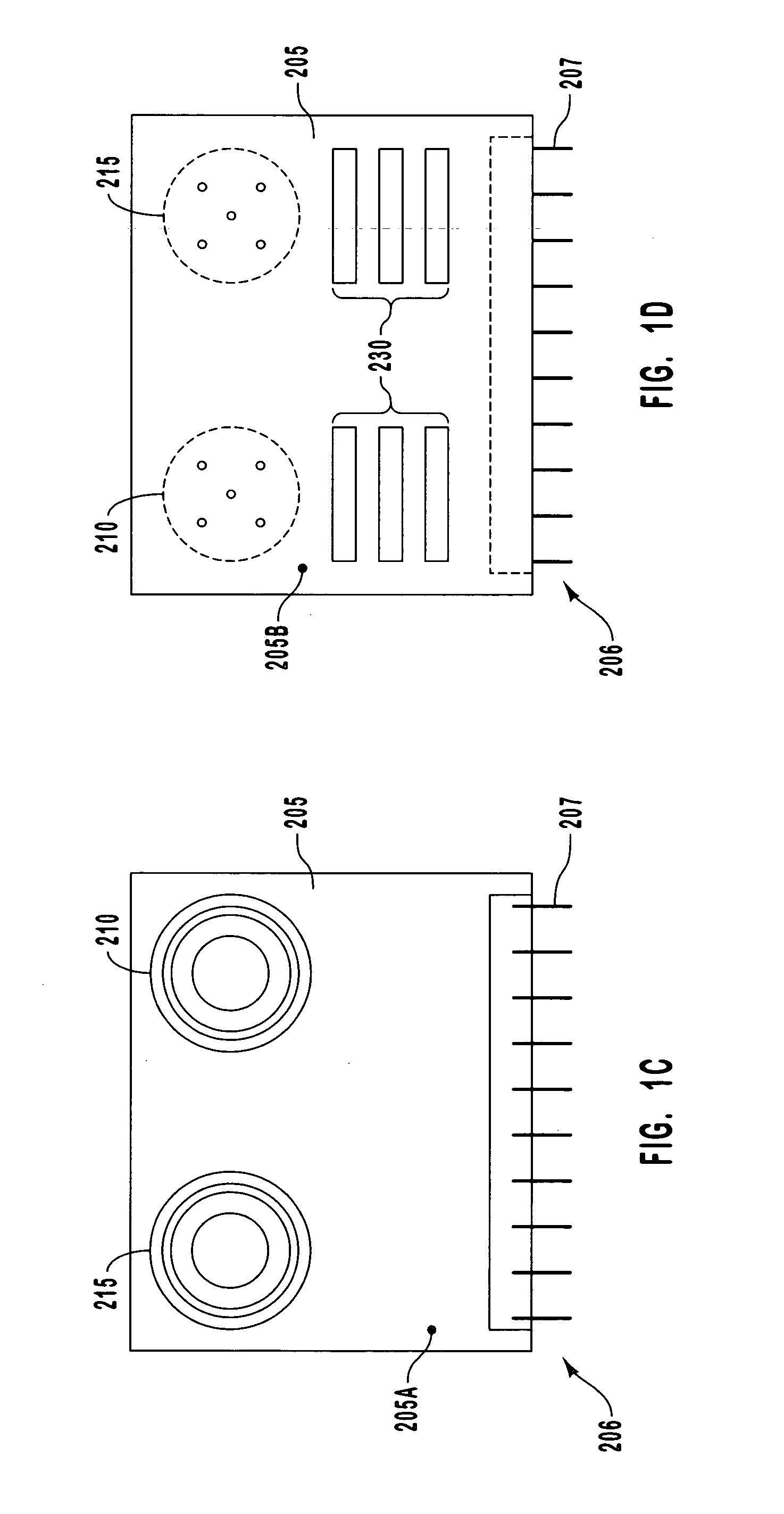
[0018] In general, exemplary embodiments of the present invention relate to compact optical transceivers that can be integrated within the relatively small physical envelopes defined by compact components, such as an HBA for use with a desktop computer, a laptop computer, or other similar computer system, while maintaining compliance with applicable operational and performance standards.

[0019] In one exemplary implementation, an optical transceiver is provided that comprises a transceiver housing wherein a ROSA and a TOSA reside. The ROSA and TOSA each define a longitudinal axis, and a transceiver substrate is mounted within the housing in a plane that is substantially perpendicular to the longitudinal axes respectively defined by the ROSA and TOSA. The transceiver substrate includes a plurality of electrical connections configured and arranged to operably interact with corresponding connections of an HBA or other compact device to which the transceiver is mounted.

[0020] As a resu...


PUM


Abstract

An optical transceiver is provided that includes a transceiver substrate arranged substantially perpendicular to longitudinal axes respectively defined by a transmit optical subassembly and receive optical subassembly. The transceiver substrate is configured to electrically and physically connect to the transmit optical subassembly and the receive optical subassembly, and includes a connector configured and arranged to interface with a host bus adapter. The combination of the host bus adapter and optical transceiver is sized and configured to be received within a standard slot of a host system, such as a PCI or PCMCIA slot. In this way, one or more optical connections are integrated within the host device or system.

Description

CROSS-REFERENCE TO RELATED APPLICATIONS [0001] This application claims the benefit of U.S. Provisional Patent Application Ser. No. 60 / 520,885 filed on Nov. 17, 2003, entitled “COMPACT OPTICAL TRANSCEIVERS FOR HOST BUS ADAPTERS,” incorporated herein in its entirety by this reference.BACKGROUND OF THE INVENTION [0002] 1. The Field of the Invention [0003] This invention relates generally to optical transceivers. More specifically, exemplary embodiments of the invention are concerned with optical transceivers configured to be implemented within relatively compact components, such as host bus adapters, while maintaining compliance with established form factors and other standards. [0004] 2. Related Art [0005] Fiber optic technology is increasingly employed as a method by which information can be reliably transmitted via a communications network. Networks employing fiber optic technology are known as optical communications networks, and are marked by high bandwidth and reliable, high-spee...

Claims


Application Information

Patent Timeline
Patent Type & Authority Applications(United States)
IPC IPC(8): G02B6/42H05K1/14H05K3/36
CPCG02B6/4292H05K1/141H05K2201/10189H05K2201/10121H05K3/366
Inventor LIGHT, GRETA
Owner II VI DELAWARE INC
Why Eureka
Try Eureka