Single package containing multiple integrated circuit devices

a technology of integrated circuit devices and single devices, which is applied in the field of single package containing multiple integrated circuit devices, can solve the problems of dc to dc, the spacing requirements of internal ic devices to maintain a small package footprint, and the inability to meet the requirements of spacing between internal ic devices

Inactive Publication Date: 2005-04-19
TAIWAN SEMICON MFG CO LTD
View PDF11 Cites 45 Cited by
  • Summary
  • Abstract
  • Description
  • Claims
  • Application Information

AI Technical Summary

Benefits of technology

[0006]The present invention allows multiple IC devices to be placed on the same substrate within a single BGA package. The invention requires minimum distances to be kept between electrical connections of the IC devices to ma...

Problems solved by technology

The IC devices within such simple packages are limited to simple transceivers and DC to DC converters, and such packages are limited to DIP (dual in package), SOJ (small outline J lead), QFP (quad flat package) and high QFP.
Such efforts, however, have not prov...

Method used


Image

  • Single package containing multiple integrated circuit devices
  • Single package containing multiple integrated circuit devices
  • Single package containing multiple integrated circuit devices

Examples


Embodiment Construction

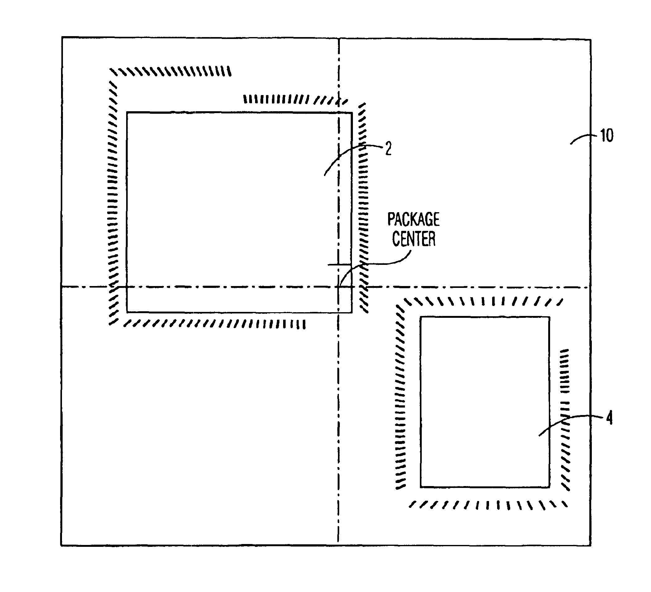
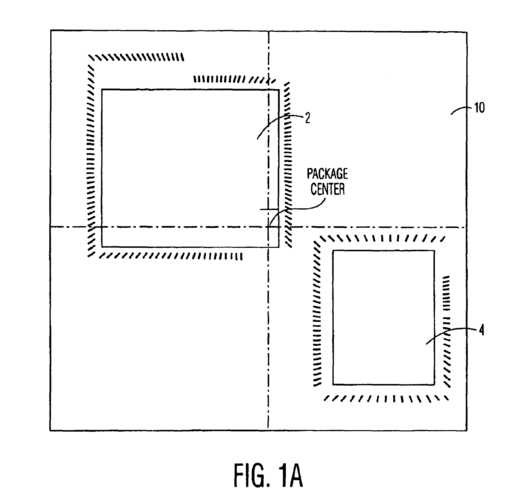
[0022]FIG. 1A shows a layout of two IC devices 2 and 4 inside a ball grid array (BGA) package 10 according to one embodiment of the invention. These devices are placed on the same package substrate in package 10 and are electrically isolated from each other. In this exemplary layout, device 2 may be a L41 chip, which is a 1394a Link Layer Controller with copy protection and device 4 may be a P23 chip, which is 1394a Physical Layer Controller with two ports. Both L41 and P23 chips are available from Philips Semiconductors, Inc., Sunnyvale, Calif.

[0023]According to the invention, each IC device should be placed on the package substrate in an orientation that allows segregation of the electrical connections of the IC devices placed at specific areas. For example, two IC devices would be placed in two different sections as in FIG. 1A; three IC devices would be placed in three different sections, etc. Furthermore, the electrical connections of the devices on the substrate are maintained ...


PUM


Abstract

The present invention allows multiple IC devices to be placed on the same substrate within a single BGA package. The invention requires minimum distances to be kept between electrical connections of the IC devices to maintain the electrical isolation, so that the devices can be operated at different voltage differentials. Signals between the devices can be connected externally from the package to each other utilizing galvanic isolation techniques. The invention provides the flexibility of choice for the customers to use isolation or not between the devices and takes up less PC board space because only a single package is used on the board.

Description

[0001]This application claims the benefit of U.S. Provisional Application No. 60 / 304,038, filed on Jul. 9, 2001.BACKGROUND OF THE INVENTION[0002]The invention relates generally to semiconductor integrated circuit (IC) packages and more particularly, it relates to an improved ball grid array (BGA) package which contains multiple IC devices electrically isolated from each other.[0003]Conventionally, IC devices are mounted on a PC board and electrical isolation of the IC devices is maintained on the board. In order to efficiently use spaces on the PC board, there are packages which contain multiple IC devices, commonly referred to as multi-chip modules (MCM's). These devices are connected to each other inside the package and share both the power and ground levels. Simple packages, which contain two IC devices and maintain them electrically isolated within a single package, are also used. The IC devices within such simple packages are limited to simple transceivers and DC to DC converte...

Claims


Application Information

Patent Timeline
IPC IPC(8): H01L23/52H01L23/538H01L25/065H05K3/34H05K1/14H01L25/10H01L25/18
CPCH01L23/5386H01L25/0655H01L2224/16225H05K1/141H05K3/3436H01L2924/15311H01L23/48
Inventor DAVENPORT, JOEL WAYNEPARKER, ROBERT R.CONDER, JEFF E.
Owner TAIWAN SEMICON MFG CO LTD
Why Eureka
Try Eureka