NANOWIRE METAL-OXIDE SEMICONDUCTOR (MOS) FIELD-EFFECT TRANSISTORS (FETs) (MOSFETs) EMPLOYING A NANOWIRE CHANNEL STRUCTURE EMPLOYING RECESSED CONDUCTIVE STRUCTURES FOR CONDUCTIVELY COUPLING NANOWIRE STRUCTURES

a metal-oxide semiconductor and nanowire technology, applied in the field of metal-oxide semiconductor (mos) field-effect transistors (fets) (mosfets), can solve the problems of increasing gate resistance, reducing electrostatic control of the channel, increasing the delay of the nanowire mosfet, etc., to reduce leakage current, increase drive strength, and small channel length

Inactive Publication Date: 2017-07-20
QUALCOMM INC
View PDF2 Cites 22 Cited by
  • Summary
  • Abstract
  • Description
  • Claims
  • Application Information

AI Technical Summary

Benefits of technology

[0009]Aspects of the present disclosure involve nanowire metal-oxide semiconductor (MOS) Field-Effect Transistors (FETs) (MOSFETs) employing a nanowire channel structure employing recessed conductive structures for conductively coupling nanowire structures. The use of a nanowire channel structure in a MOSFET provides for an effective smaller channel length as compared to planar transistors to increase drive strength with strong electrostatic gate control of the channel to reduce leakage current. To increase the effective channel width of the nanowire channel structure for increased drive strength (i.e., drive current), multiple nanowire structures can be provided and vertically stacked in a nanowire channel structure in a nanowire MOSFET to increase channel current density for a given nanowire channel structure height. Scaling down the vertical space between adjacent, vertically stacked nanowire structures in a nanowire channel structure also reduces parasitic capacitances, thereby reducing delay of the nanowire MOSFET and increasing frequency performance as a result. However, there is a minimum distance required between adjacent nanowire structures due to fabrication limitations to allow gate material to be disposed to surround the adjacent nanowire structures to provide sufficient electrostatic control of the channel. Thus, scaling down the vertical space between adjacent, vertically stacked nanowire structures in a nanowire channel structure can decrease the amount of gate material provided in the nanowire channel structure for a given height, thereby reducing electrostatic control of the channel and increasing gate resistance, which increases delay of the nanowire MOSFET.
[0010]In this regard, to provide for multiple vertically stacked nanowire structures in a nanowire channel structure to increase drive strength, but with a reduced gate resistance and a relaxation of the distance between adjacent nanowire structures to ease the gate material filling process, nanowire MOSFETs employing a nanowire channel structure employing conductive structures conductively coupled to the nanowire structures are provided. The conductive structures are disposed in an area between adjacent nanowire structures in the nanowire channel structure that would otherwise be left void and subsequently filled in with gate material. The conductive structures provide an effective conductive “bridge” between adjacent nanowire structures to conductively couple the nanowire structures together in the nanowire channel structure. Providing the conductive structures in the nanowire channel structure increases the average cross-sectional area of the nanowire structures, as compared to a similar nanowire channel structure not employing the conductive structures, thus increasing the effective channel width and drive strength (i.e., drive current) for a given channel structure height. The precision of a gate material filling process is also eased, because the gate material does not have to be disposed in the areas between adjacent nanowire structures occupied by the conductive structures. Thus, the nanowire structures may be located closer to each other to provide a greater effective channel width and drive strength without having to increase the height of the nanowire channel structure. The width of the conductive structures can also be recessed with regard to the width of the nanowire structures in the nanowire channel structure to allow for a thicker metal gate to lower gate resistance, while still providing excellent electrostatic gate control of the channel.

Problems solved by technology

However, there is a minimum distance required between adjacent nanowire structures due to fabrication limitations to allow gate material to be disposed to surround the adjacent nanowire structures to provide sufficient electrostatic control of the channel.
Thus, scaling down the vertical space between adjacent, vertically stacked nanowire structures in a nanowire channel structure can decrease the amount of gate material provided in the nanowire channel structure for a given height, thereby reducing electrostatic control of the channel and increasing gate resistance, which increases delay of the nanowire MOSFET.

Method used


Image

  • NANOWIRE METAL-OXIDE SEMICONDUCTOR (MOS) FIELD-EFFECT TRANSISTORS (FETs) (MOSFETs) EMPLOYING A NANOWIRE CHANNEL STRUCTURE EMPLOYING RECESSED CONDUCTIVE STRUCTURES FOR CONDUCTIVELY COUPLING NANOWIRE STRUCTURES
  • NANOWIRE METAL-OXIDE SEMICONDUCTOR (MOS) FIELD-EFFECT TRANSISTORS (FETs) (MOSFETs) EMPLOYING A NANOWIRE CHANNEL STRUCTURE EMPLOYING RECESSED CONDUCTIVE STRUCTURES FOR CONDUCTIVELY COUPLING NANOWIRE STRUCTURES
  • NANOWIRE METAL-OXIDE SEMICONDUCTOR (MOS) FIELD-EFFECT TRANSISTORS (FETs) (MOSFETs) EMPLOYING A NANOWIRE CHANNEL STRUCTURE EMPLOYING RECESSED CONDUCTIVE STRUCTURES FOR CONDUCTIVELY COUPLING NANOWIRE STRUCTURES

Examples


Embodiment Construction

[0030]With reference now to the drawing figures, several exemplary aspects of the present disclosure are described. The word “exemplary” is used herein to mean “serving as an example, instance, or illustration.” Any aspect described herein as “exemplary” is not necessarily to be construed as preferred or advantageous over other aspects.

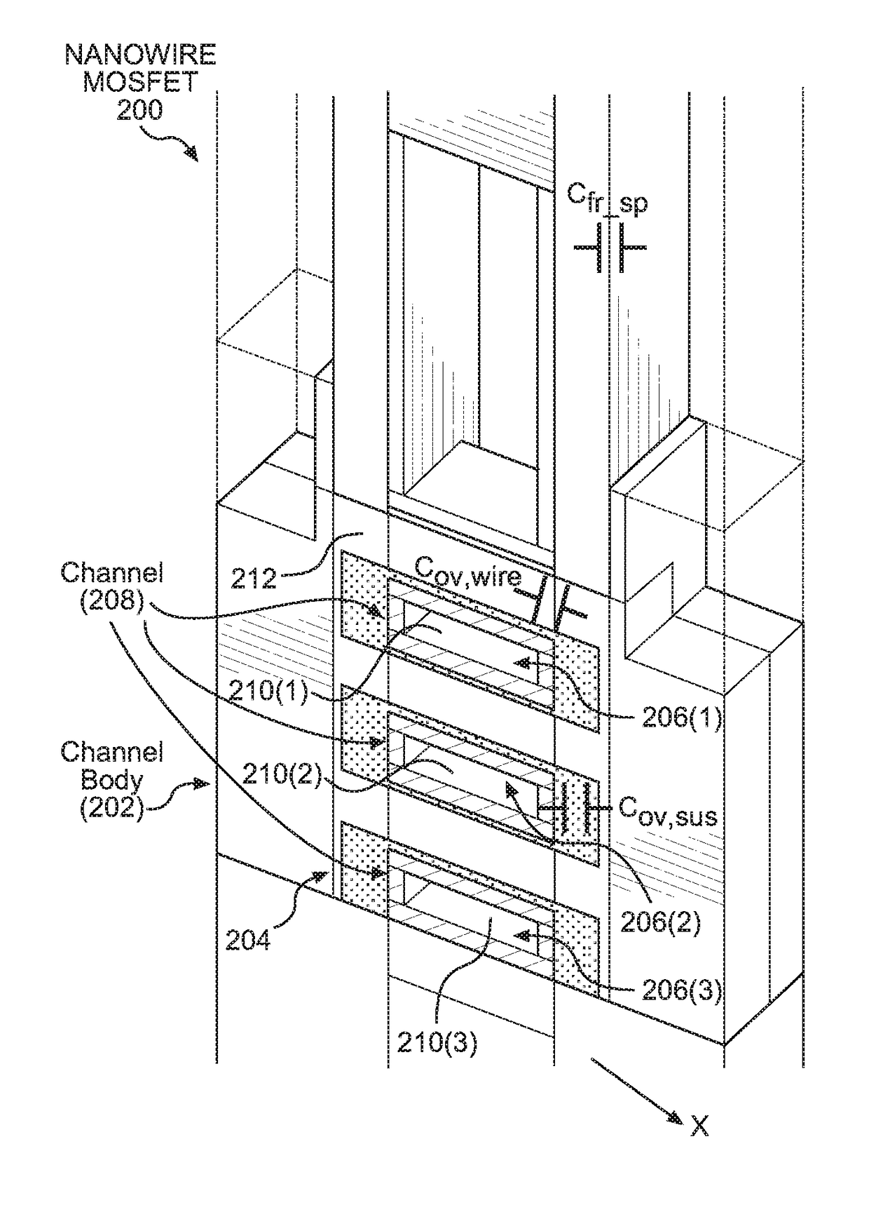
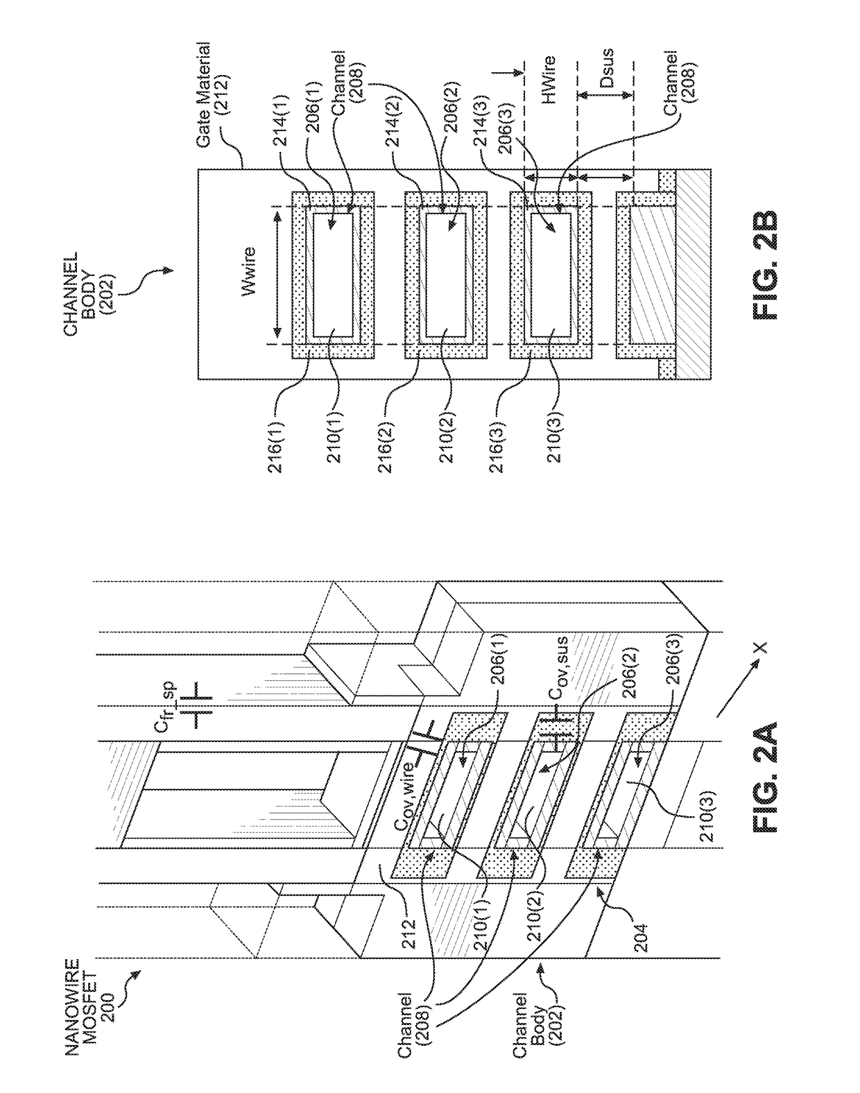
[0031]Aspects of the present disclosure involve nanowire metal-oxide semiconductor (MOS) Field-Effect Transistors (FETs) (MOSFETs) employing a nanowire channel structure employing recessed conductive structures for conductively coupling nanowire structures. The use of a nanowire channel structure in a MOSFET provides for an effective smaller channel length as compared to planar transistors to increase drive strength with strong electrostatic gate control of the channel to reduce leakage current. To increase the effective channel width of the nanowire channel structure for increased drive strength (i.e., drive current), multiple nanowire structures can...


PUM

PropertyMeasurementUnit
widthaaaaaaaaaa
widthaaaaaaaaaa
sizesaaaaaaaaaa

Abstract

Nanowire metal-oxide semiconductor (MOS) Field-Effect Transistors (FETs) (MOSFETs) employing a nanowire channel structure employing recessed conductive structures for conductively coupling nanowire structures are disclosed. Conductive structures are disposed between adjacent nanowire structures to conductively couple nanowire structures. Providing conductive structures in the nanowire channel structure increases the average cross-sectional area of nanowire structures, as compared to a similar nanowire channel structure not employing conductive structures, thus increasing effective channel width and drive strength for a given channel structure height. The precision of a gate material filling process is also eased, because gate material does not have to be disposed in areas between adjacent nanowire structures occupied by conductive structures. The conductive structure width can also be recessed with regard to width of nanowire structures in the nanowire channel structure to allow for a thicker metal gate to lower the gate resistance, while providing excellent electrostatic gate control of the channel.

Description

PRIORITY APPLICATION[0001]The present application claims priority under 35 U.S.C. §119(e) to U.S. Provisional Patent Application Ser. No. 62 / 279,217 filed on Jan. 15, 2016, and entitled “NANOWIRE METAL-OXIDE SEMICONDUCTOR (MOS) FIELD-EFFECT TRANSISTORS (FETs) (MOSFETs) EMPLOYING A NANOWIRE CHANNEL STRUCTURE EMPLOYING CONDUCTIVELY COUPLED NANOWIRE STRUCTURES,” the contents of which is incorporated herein by reference in its entirety.BACKGROUND[0002]I. Field of the Disclosure[0003]The technology of the disclosure relates generally to metal-oxide semiconductor (MOS) Field-Effect Transistors (FETs) (MOSFETs), and more particularly to the use of nanowire channels (e.g., silicon nanowires) in MOSFETs for short channel control.[0004]II. Background[0005]Transistors are essential components in modern electronic devices. Large numbers of transistors are employed in integrated circuits (ICs) in many modern electronic devices. For example, components such as central processing units (CPUs) and ...

Claims


Application Information

Patent Timeline
Patent Type & Authority Applications(United States)
IPC IPC(8): H01L29/423H01L29/66H01L29/78
CPCH01L29/42392H01L29/66795H01L29/785H01L29/0673H01L29/66439H01L29/66484H01L29/775H01L29/7831
Inventor SONG, STANLEY SEUNGCHULXU, JEFFREY JUNHAORIM, KERNYANG, DAFENG, PEIJIEYEAP, CHOH FEI
Owner QUALCOMM INC
Why Eureka
Try Eureka