Method for mounting semiconductor chip and semiconductor chip-mounted board

a technology of semiconductor chip and mounting board, which is applied in the direction of semiconductor devices, semiconductor/solid-state device details, electrical apparatus, etc., can solve the problems of increasing the duration of bonding, difficult to reliably bond led 501/b> to the board, and becoming remarkable, so as to achieve easy deformation, high accuracy, and control the feed rate of conductive materials

Inactive Publication Date: 2005-05-26
PANASONIC CORP
View PDF21 Cites 77 Cited by
  • Summary
  • Abstract
  • Description
  • Claims
  • Application Information

AI Technical Summary

Benefits of technology

[0020] Accordingly, the object of the present invention is to solve the aforementioned problems and provide a semiconductor chip mounting method capable of carrying out reliable efficient bonding while reducing the occurrence of defective bonding caused by the application of ultrasonic vibrations in mounting a semiconductor chip on a board by bonding chip-electrodes of the semiconductor chip to board-electrodes of the board by applying the ultrasonic vibrations, and a semiconductor chip-mounted board.
[0071] Moreover, an effect similar to the above effect can be obtained-even when protruding electrodes are formed on the chip-electrodes of the semiconductor chip or the board-electrodes of the board.

Problems solved by technology

In the above cases, there is a problem that it becomes difficult to reliably bond the LED 501 to the board 503.
This alloy layer 505a has a characteristic that it is hard and fragile in comparison with the bumps formed of gold, and therefore, stress concentration might occur in the main body of the LED 501 due to the application of the ultrasonic vibrations, possibly causing cracks in the LED 501.
Particularly, such a problem becomes remarkable with an increase in the duration of bonding when the bumps 501 of a large size are used.

Method used


Image

  • Method for mounting semiconductor chip and semiconductor chip-mounted board
  • Method for mounting semiconductor chip and semiconductor chip-mounted board
  • Method for mounting semiconductor chip and semiconductor chip-mounted board

Examples


first embodiment

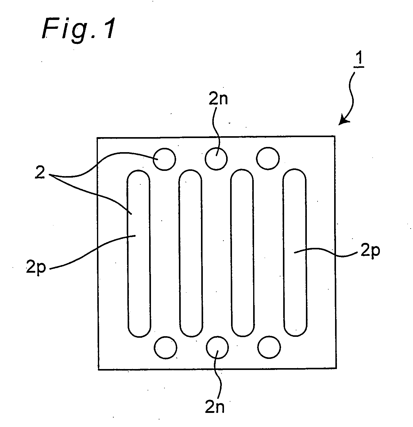
[0092] In connection with a semiconductor chip mounting method according to the first embodiment of the present invention, FIG. 1 shows a schematic explanatory view illustrating the planar structure of an LED chip (or an LED device) to be mounted on a board of one example of the semiconductor chip.

[0093] As shown in FIG. 1, the LED (Light Emitting Diode) chip 1 has an approximate square shape, and a plurality of pads 2 of one example of the chip-electrodes are formed on the bonding side surface of the board. The pads 2 are formed separated into two kinds of P-pole pads (one example of the P-type electrode) 2p formed into an elliptic shape and N-pole pads (one example of the N-type electrode) 2n formed into an approximate circle shape according to the characteristics of the LED chip 1. For example, each of the P-pole pads 2p is formed in a size of about 0.6 mm×0.1 mm, and each of the N-pole pads 2n is formed in a size of a diameter of about 0.1 mm.

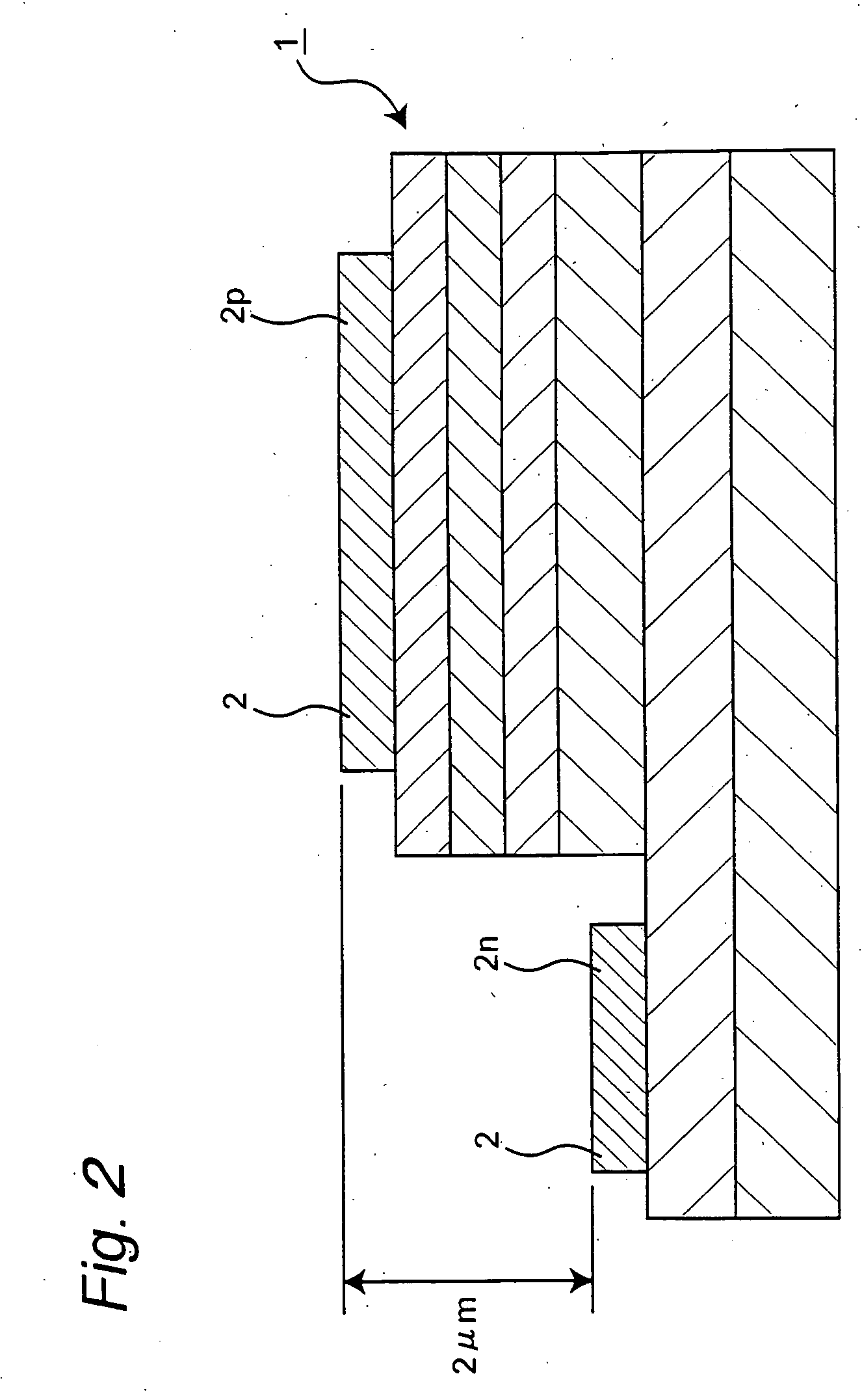
[0094] Moreover, FIG. 2 shows a sc...

second embodiment

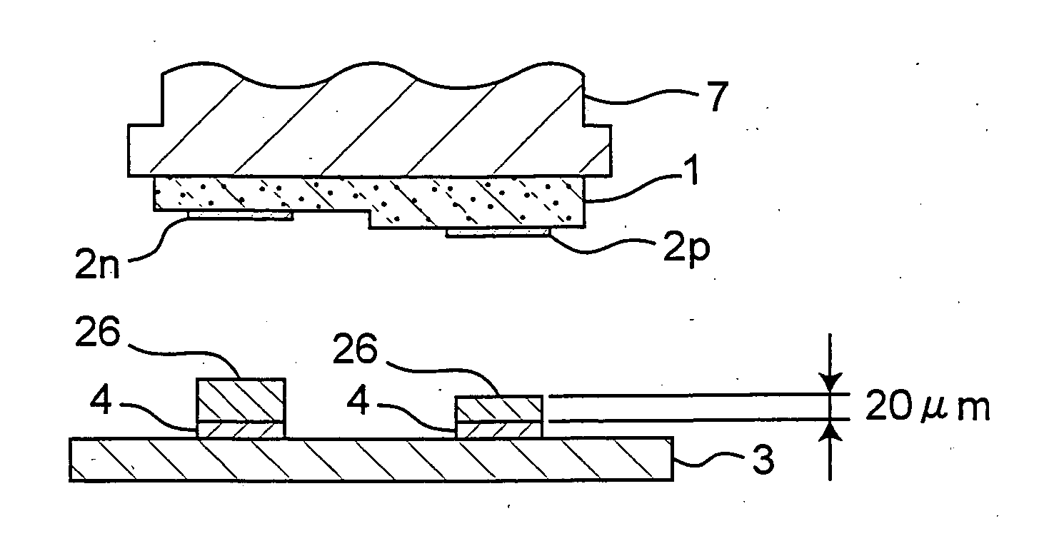
[0126] The present invention is not limited to the above embodiment but allowed to be implemented in various forms. For example, a mounting method of the LED chip 1 of one example of the semiconductor chip mounting method according to a second embodiment of the present invention will be described with reference to the schematic explanatory views shown in FIG. 5. The same constituents as those owned by the LED chip 1 and the board 3 of the first embodiment are denoted by the same reference numerals for the purpose of easily understanding the explanation.

[0127] First, as shown in FIG. 5A, the bumps 5 are formed on the respective pads 2 on the upper surface of the LED chip 1 similarly to the first embodiment. The bumps 5 are formed of, for example, gold by the plating method. Moreover, since there is a difference in the formation height (e.g., a difference in the formation height of 2 μm) between the P-pole pad 2p and the N-pole pad 2n of the LED chip 1, a height difference of the sam...

third embodiment

[0136] A mounting method of the LED chip 1 of one example of the semiconductor chip mounting method according to a third embodiment of the present invention will be described with reference to the schematic explanatory views shown in FIGS. 8A, 8B and 8C. The same constituents as those owned by the LED chip 1 and the board 3 of the first embodiment are denoted by the same reference numerals for the purpose of easily understanding the explanation.

[0137] According to the third embodiment of the present invention, mounting is carried out without forming bumps instead of forming bumps on the pads 2 of the LED chip 1 by the plating method and mounting the LED chip 1 on the board 3 with interposition of the bumps as in the first embodiment and the second embodiment.

[0138] First of all, as shown in FIG. 8A, bonding electrodes 26 are formed by feeding a gold nanopaste onto the upper surfaces of the board-electrodes 4 of the board 3 by coating or printing means. At this time, the bonding el...


PUM


Abstract

By arranging bonding members formed of a gold nanopaste between chip-electrodes and board-electrodes, making the chip-electrodes are brought in contact with the respective board-electrodes via the bonding members and applying ultrasonic vibrations to the bonding members in the contact state, the bonding members are bonded to the board-electrodes and the chip-electrodes.

Description

BACKGROUND OF THE INVENTION [0001] The present invention relates to a semiconductor chip mounting method for producing a semiconductor chip-mounted board by bonding board-electrodes of a board to chip-electrodes of a semiconductor chip to mount the semiconductor chip on the board, and relates to the semiconductor chip-mounted board. [0002] Conventionally, an LED (LED chip), which is one example of the semiconductor chip, has been used for a fluorescent lamp or the like by utilizing its light-emitting function. However, the LED, which can emit light with a voltage applied thereto, has a problem that heat is generated accompanying the light emission and the luminous efficiency of the LED is reduced by the generation of heat, causing a reduction in the luminous intensity. In order to solve the problem, various devices have conventionally been invented to let the heat generated from the LED efficiently escape. [0003] For example, as one of the devices, a technique for letting heat escap...

Claims


Application Information

Patent Timeline
Patent Type & Authority Applications(United States)
IPC IPC(8): H01L21/607H01L23/485H01L23/498H01L33/62
CPCH01L23/49811H01L2224/11505H01L33/62H01L2224/0401H01L2224/0603H01L2224/1131H01L2224/1134H01L2224/1308H01L2224/13082H01L2224/13144H01L2224/13644H01L2224/1403H01L2224/16H01L2224/81192H01L2224/81194H01L2224/81205H01L2224/81801H01L2224/85424H01L2924/01004H01L2924/01013H01L2924/01015H01L2924/01033H01L2924/01078H01L2924/01079H01L2924/01082H01L2924/09701H01L24/81H01L2224/06102H01L2924/10253H01L2224/92125H01L2224/73204H01L2224/32225H01L2224/16225H01L2924/12041H01L24/16H01L24/14H01L24/13H01L24/06H01L2924/014H01L2924/0105H01L2924/01047H01L2924/01023H01L2924/01006H01L2924/00013H01L24/75H01L2924/00014H01L2224/13099H01L2924/00
Inventor NAITO, HIROYUKISHIDA, SATOSHIHAJI, HIROSHIMORIKAWA, MAKOTO
Owner PANASONIC CORP
Why Eureka
Try Eureka