Semiconductor memory device with refreshment control

a memory device and semiconductor technology, applied in the direction of information storage, static storage, digital storage, etc., can solve the problems of increasing peak consumption current and method not being able to reduce average consumption current, so as to achieve the effect of reducing consumption current, reducing peak consumption current, and reducing average consumption curren

Inactive Publication Date: 2005-05-26
LONGITUDE SEMICON S A R L
View PDF5 Cites 22 Cited by
  • Summary
  • Abstract
  • Description
  • Claims
  • Application Information

AI Technical Summary

Benefits of technology

[0017] Another object of the present invention is to provide a semiconductor memory device in which consumption current can be reduced in a refreshing operation.
[0018] Anot

Problems solved by technology

When the memory capacity is increased while keeping the refresh command time tRFC to a certain time period, the number of memory cells to be refre

Method used


Image

  • Semiconductor memory device with refreshment control
  • Semiconductor memory device with refreshment control
  • Semiconductor memory device with refreshment control

Examples


first embodiment

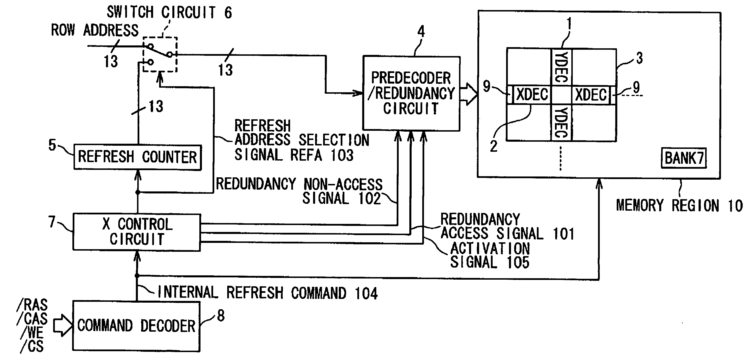
[0044]FIG. 4 is a block diagram showing the configuration of the semiconductor memory device according to the first embodiment of the present invention. The semiconductor memory device according to the embodiment includes a predecoder / redundancy circuit 4, a refresh counter 5, a switch circuit 6, an X control circuit 7, a command decoder 8, and a memory region 10. In the first embodiment, the memory region 10 has the same configuration as described with reference to FIG. 2. Namely, the memory region 10 has eight BANKs 0 to 7. Each bank includes four blocks 3, a Y decoder YDEC 1, an X decoder XDEC 2, memory cell arrays containing memory sub arrays, and a control signal generating circuit 9. The Y decoder YDEC 1 is arranged between two blocks 3 adjacent in a left and right direction to select a pair of bit lines. The X decoder XDEC 2 for word line selection, the control signal generating circuit 9, and an amplifier (not shown) for amplification of input / output data are arranged betwee...


PUM


Abstract

A semiconductor memory device includes a pair of memory sub arrays and a control signal generating circuit. The pair of memory sub arrays shares a sense amplifier, and each of the pair of memory sub arrays has a plurality of memory cells arranged in a matrix. Each of columns of the matrix is connected to a pair of bit lines, and each of rows of the matrix is connected to a word line. The control signal generating circuit sequentially outputs first and second refresh start signals within an operation time to an external refresh command in response to an internal refresh command. A first refreshing operation is carried out to first memory cells connected to a first word line of one of the memory sub arrays in response to the first refresh start signal, and a second refreshing operation is carried out to second memory cells connected to a second word line different from the first word line in the memory sub array in response to the second refresh start signal.

Description

BACKGROUND OF THE INVENTION [0001] 1. Field of the Invention [0002] The present invention relates to a semiconductor memory device and in particular to a refreshing technique in a semiconductor memory device. [0003] 2. Description of the Related Art [0004] Increase in the memory capacity and miniaturization in processes progress in semiconductor memory devices such as DRAM. Thus, the number of memory cells to be refreshed is also increasing with the increase in the memory capacity. The refreshing operation is carried out in response to a refresh command, and a time period between the refresh commands is defined by tRFC (hereinafter, referred to as “refresh command time”). When the memory capacity is increased while keeping the refresh command time tRFC to a certain time period, the number of memory cells to be refreshed per unit time increases, resulting in increase in peak consumption current. For this reason, the specification of DRAM have been standardized in such a manner that t...

Claims


Application Information

Patent Timeline
IPC IPC(8): G11C11/406G11C11/407G11C29/00
CPCG11C11/406G11C29/783G11C11/40618G11C11/40611
Inventor DONO, CHIAKIKOSHIKAWA, YASUJI
Owner LONGITUDE SEMICON S A R L
Why Eureka
Try Eureka