Solid-state imaging device

a solid-state imaging and imaging device technology, applied in the direction of color television, television systems, radio control devices, etc., can solve the problem of difficult to fix the intermediate portion of the p-well at a ground potential, and achieve the effect of suppressing the shading of the output signal and minimizing the increase in the dimensions of the pixel

Active Publication Date: 2005-06-02
SONY CORP
View PDF5 Cites 33 Cited by
  • Summary
  • Abstract
  • Description
  • Claims
  • Application Information

AI Technical Summary

Benefits of technology

[0022] In order to solve the above problems, an object of the present invention is to provide a solid-state imaging device capable of minimizing an increase in the dimensions of a pixel and suppressing shading of an output signal due to a variation in the potential of a well.

Problems solved by technology

However, for the structure in which a well contact part is disposed only at the periphery of the pixel array area, if an increase in the number of pixels increases the dimensions of P-wells of a pixel array area, it is difficult to fix the intermediate portion of the P-wells at a ground potential.
Thus, the following problems occur.

Method used


Image

  • Solid-state imaging device
  • Solid-state imaging device
  • Solid-state imaging device

Examples


first embodiment

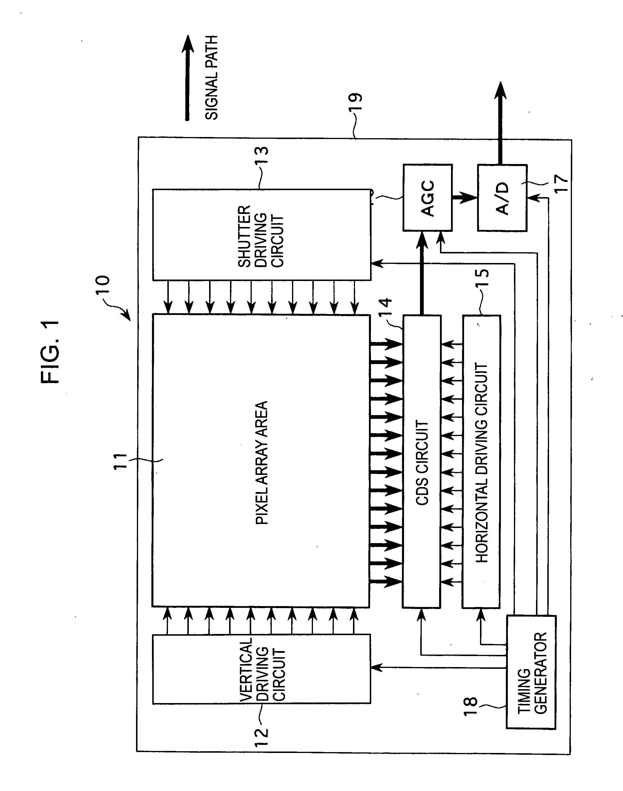
[0052] According to a first embodiment of the present invention, in a solid-state imaging device, such as a CMOS image sensor having the arrangement shown in FIG. 1, by achieving well contact in an activation region of a photoelectric conversion portion for each pixel in the pixel array area 11, an increase in the dimensions of a unit pixel (the size of a pixel) is minimized and shading of an output signal due to a variation in the potential of a well is suppressed.

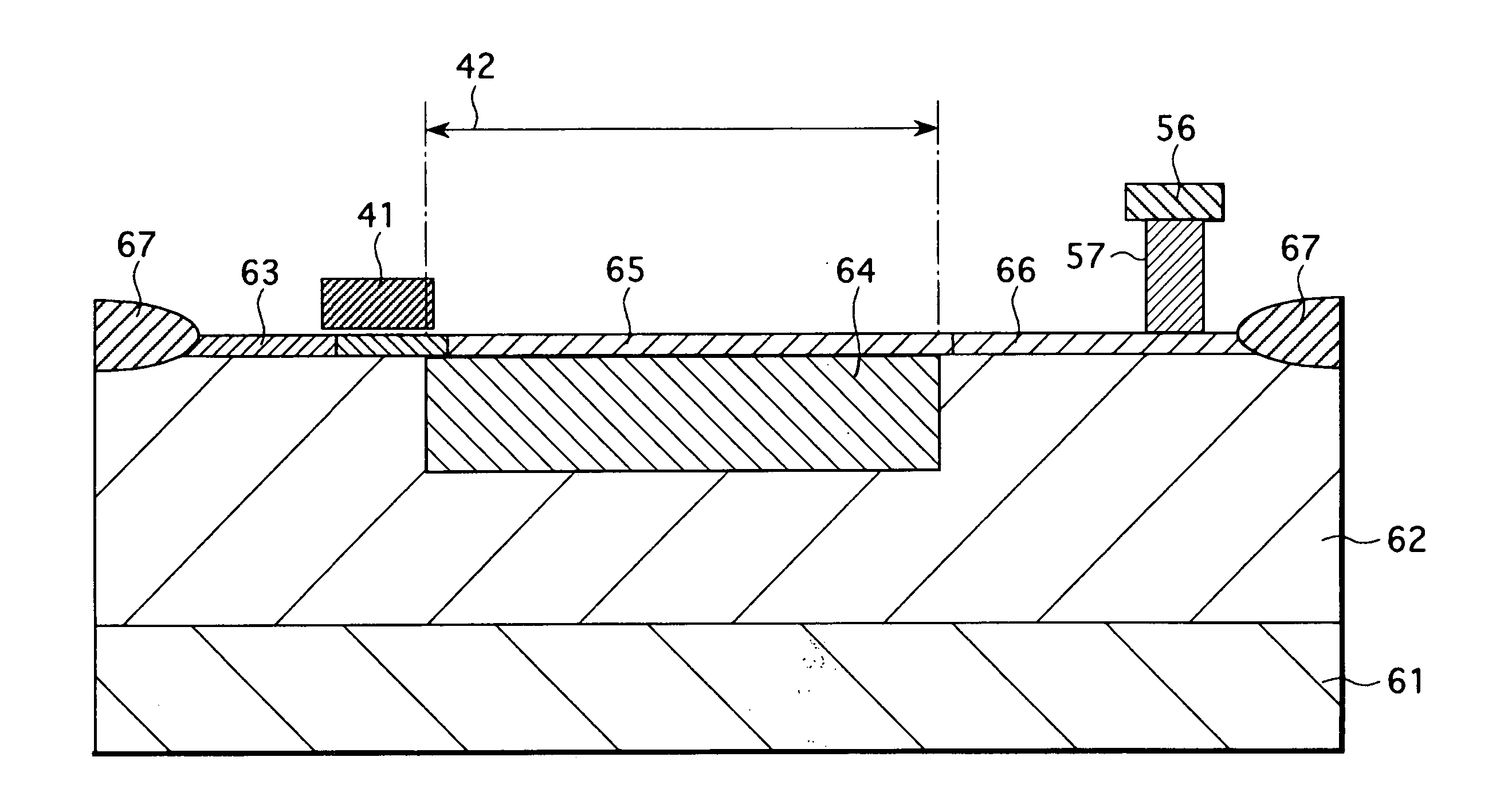
[0053]FIG. 3 is a plan pattern view showing a pixel structure according to the first embodiment. In FIG. 3, parts equivalent to those in FIG. 2 are represented by the same reference numerals.

[0054] Referring to FIG. 3, a gate electrode 41 is disposed between a photoelectric conversion region (activation region) 42 and an activation region 43 of the photoelectric conversion portion 21, and constitutes the transfer transistor 22. The activation region 43 is a drain region of the transfer transistor 22, a source region of ...

second embodiment

[0063] According to a second embodiment of the present invention, in a solid-state imaging device, such as a CMOS image sensor having the arrangement shown in FIG. 1, by achieving well contact for a plurality of adjoining pixels, instead of for each pixel, a reduction in the characteristics, more specifically, reductions in the saturation level and the sensitivity of the pixel can be suppressed. Specific examples will be described below.

first example

[0064]FIG. 5 is a plan view schematically showing the arrangement of a pixel array area 11A according to a first example of the second embodiment. Here, in order to simplify the drawing, the pixel array area 11A has a pixel arrangement of five rows and six columns.

[0065] As shown in FIG. 5, in the pixel array area 11A according to the first example, a plurality of adjoining pixels, for examples, four pixels, pixels 20A to 20D, constitute a unit cell 70A. A well contact part 71 is provided in the unit cell 70A for the pixels 20A to 20D without changing the size of each pixel. More specifically, rectangular corners, which are adjacent to each other, of the pixels 20A to 20D are evenly cut off, and the well contact part 71 is formed at the intermediate portion of the pixels 20A to 20D. Also, well potential fixing wires 72 each supplying a well potential to the well contact part 71 are arranged in every two columns (or every two rows), and are each electrically connected to the well co...


PUM


Abstract

A solid-state imaging device having an arrangement in which well contact is achieved for each pixel is provided. In the solid-state imaging device, a well contact part is formed in an activation region of a photoelectric conversion portion. The well contact part fixes a well in which the photoelectric conversion portion and transistors of the pixel are provided at a predetermined potential.

Description

BACKGROUND OF THE INVENTION [0001] 1. Field of the Invention [0002] The present invention relates to solid-state imaging devices, and more particularly, to a solid-state imaging device, such as a complementary metal-oxide semiconductor (CMOS) image sensor including amplifying elements for respective pixels. [0003] 2. Description of the Related Art [0004] Solid-state imaging devices need a great number of pixels arranged in a two-dimensional array fashion in a pixel array area. For example, in known CMOS image sensors, each element of a pixel is disposed in a well and the well is electrically fixed to the periphery of the pixel array area. [0005]FIG. 12 is a circuit diagram showing an example of the arrangement of a unit pixel 100. As shown in FIG. 12, the unit pixel 100 includes a photoelectric conversion portion 101, a transfer transistor 102, an amplifying transistor 103, a reset transistor 104, and a selection transistor 105. The anode of the photoelectric conversion portion 101 ...

Claims


Application Information

Patent Timeline
Patent Type & Authority Applications(United States)
IPC IPC(8): H01L27/146H01L27/14H01L31/10H04N5/335H04N5/361H04N5/369H04N5/374
CPCH01L27/14609H01L27/14603H01L27/146H04N25/76H01L27/14643
Inventor ABE, TAKASHISUZUKI, RYOJIMABUCHI, KEIJIIIZUKA, TESTUYAUENO, TAKAHISAHARUTA, TSUTOMU
Owner SONY CORP
Why Eureka
Try Eureka