Photovoltaic devices fabricated by growth from porous template

a photovoltaic device and template technology, applied in the field of nanostructured photovoltaic devices, can solve the problems of large aspect ratio, difficult filling of pores, and inability to use hybrid organic-inorganic, organic/organic photovoltaic devices,

Inactive Publication Date: 2005-06-09
AERIS CAPITAL SUSTAINABLE IP
View PDF12 Cites 289 Cited by
  • Summary
  • Abstract
  • Description
  • Claims
  • Application Information

AI Technical Summary

Benefits of technology

[0008] According to embodiment of the present invention a solar cell device includes two or more materials having different electron affinities. The solar cell device is characterized by an architecture where the materials are regularly arrayed and their presence alternates within dis

Problems solved by technology

Although anodized porous templates are known in the art, they have not been used in hybrid organic-inorganic, dye-sensitized or organic/organic photovoltaic devices.
Such large aspect ratios are problematic in terms of filling the pores and charge recombination within the filled pores.
For example, if a device were built using an Al layer several micrometers thick, filling the pore

Method used


Image

  • Photovoltaic devices fabricated by growth from porous template
  • Photovoltaic devices fabricated by growth from porous template
  • Photovoltaic devices fabricated by growth from porous template

Examples


Embodiment Construction

Contents

[0024] I. Glossary [0025] II. Introduction [0026] III. General Overview [0027] IV. Photovoltaic Device [0028] V. Photovoltaic Device Fabrication [0029] VI. Alternative Embodiments [0030] VII. Conclusion

I. GLOSSARY

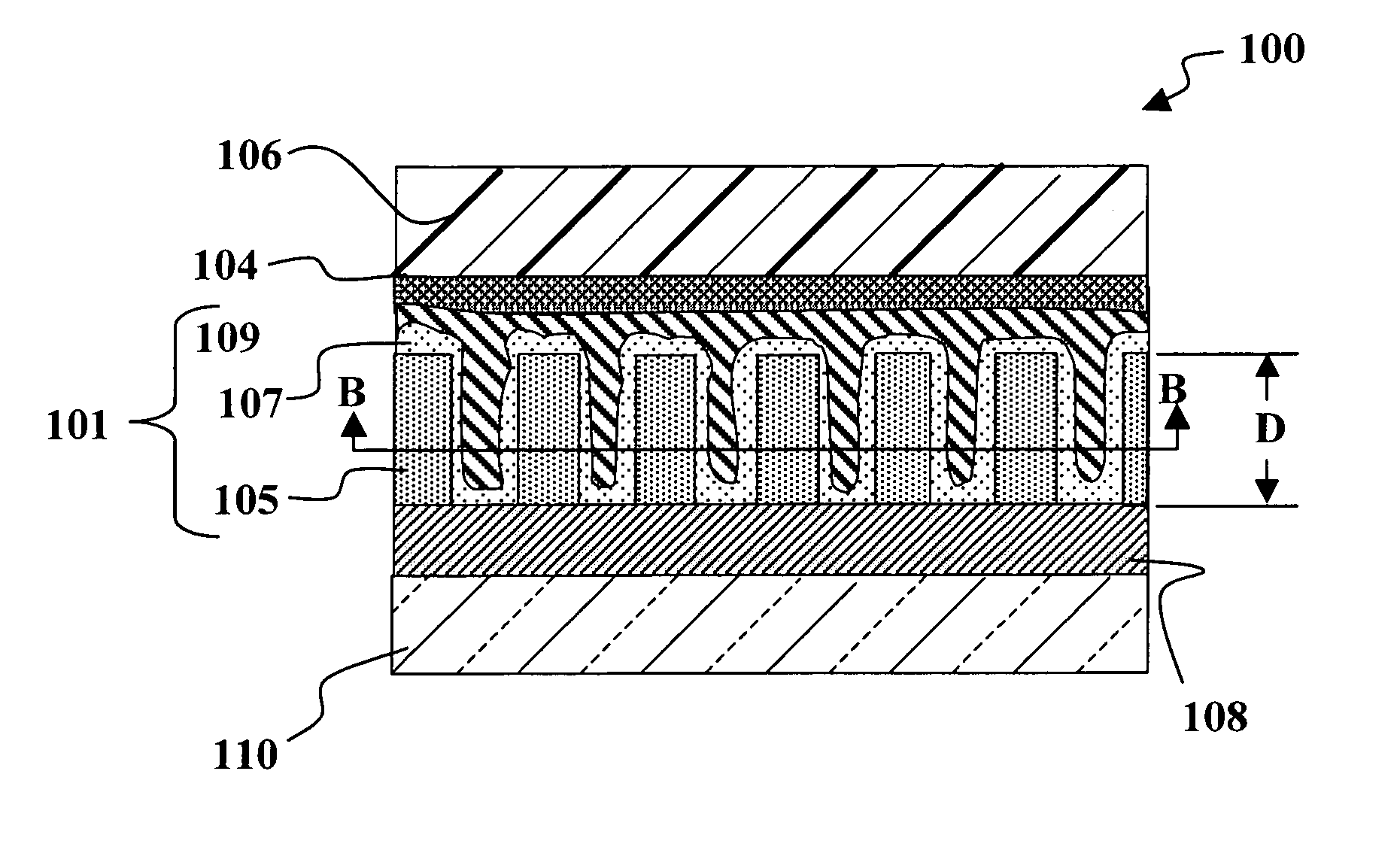
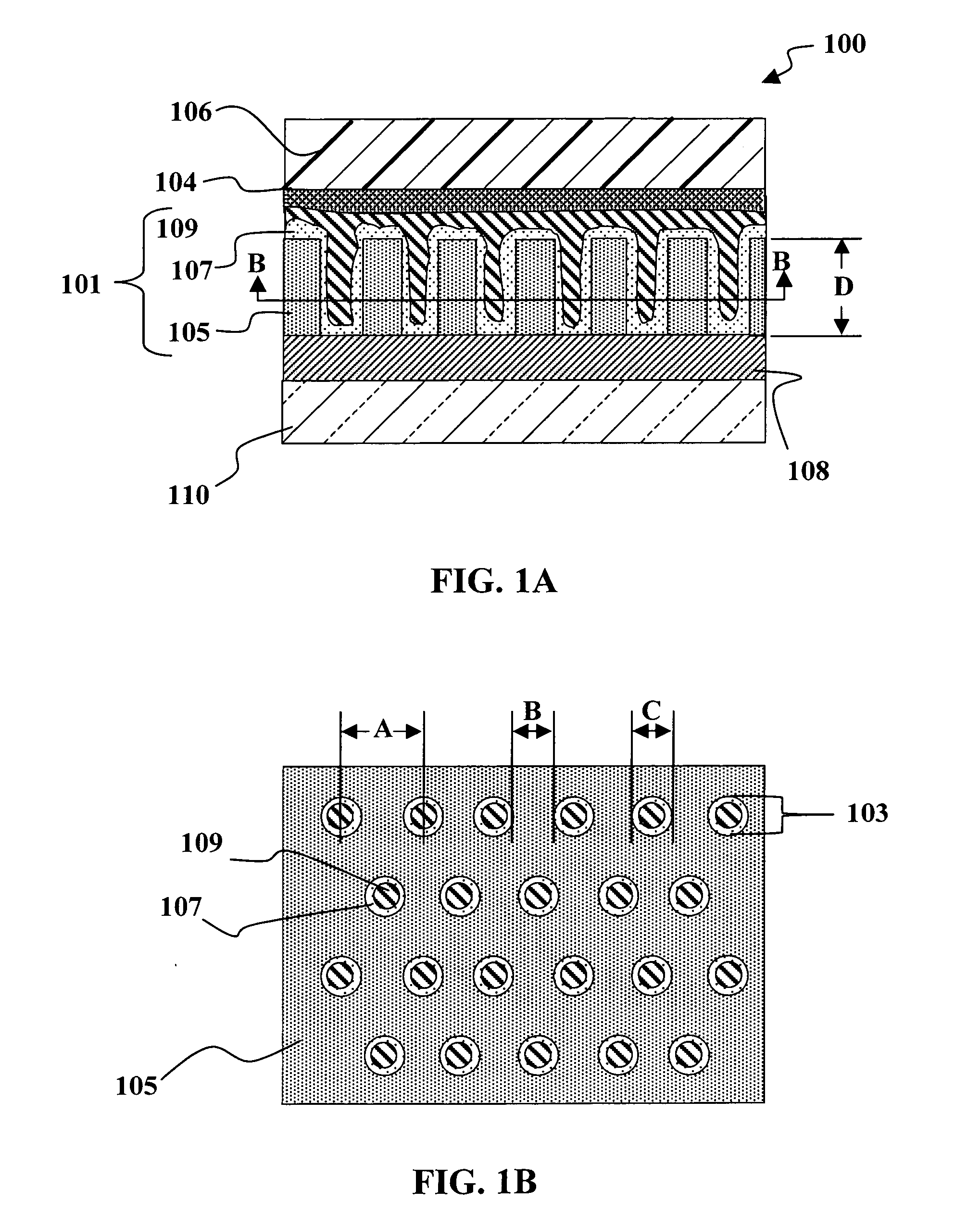
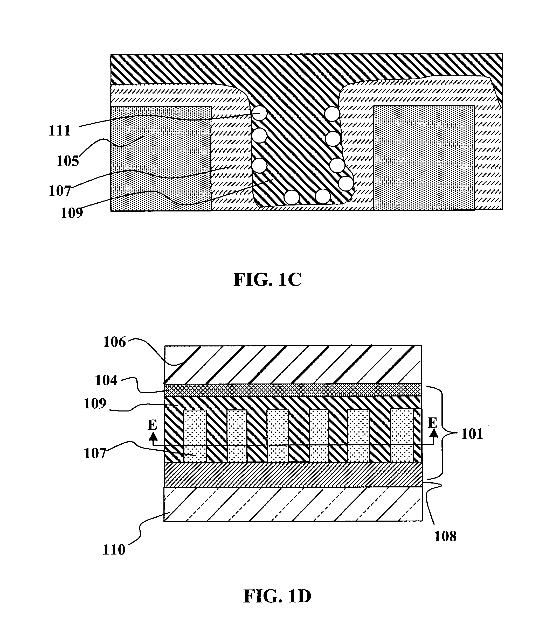
[0031] The following terms are intended to have the following general meanings as they are used herein: [0032] The article “A”, or “An” refers to a quantity of one or more of the item following the article, except where expressly stated otherwise, e.g., “a single” layer. [0033] Active Layer generally refers to the layer within a photovoltaic or solar cell device where conversion of radiant energy to electrical energy takes place. [0034] Anodization refers to the formation of a film, such as an oxide, on a conducting material, such as a metal, by electrolysis. [0035] Array refers to a regular arrangement of objects or structures over a scale of distance greater than some characteristic dimension of a typical structure or object in the array. [0036] Aspect Ratio: ...


PUM

PropertyMeasurementUnit
Thicknessaaaaaaaaaa
Thicknessaaaaaaaaaa
Thicknessaaaaaaaaaa

Abstract

Photovoltaic devices, such as solar cells, and methods for their manufacture are disclosed. A device may be characterized by an architecture where two more materials having different electron affinities are regularly arrayed such that their presence alternates within distances of between about 1 nm and about 100 nm. The materials are present in a matrix based on a porous template with an array of template pores. The porous template is formed by anodizing a layer of metal. A photovoltaic device may include such a porous template disposed between a base electrode and a transparent conducting electrode. A first charge-transfer material fills the template pores, A second (complementary) charge-transfer material fills additional space not occupied by the first charge-transfer material.

Description

CROSS-REFERENCE TO RELATED APPLICATIONS [0001] This application is a continuation-in-part of and claims priority to commonly assigned U.S. patent application Ser. Nos. 10 / 290,119, 10 / 303,665 and 10 / 319,406, the entire disclosures of all of which are incorporated herein by reference. This application also claims priority to U.S. Provisional Patent Application 60 / 390,904, filed Jun. 22, 2002, the entire disclosures of which are incorporated herein by reference.FIELD OF THE INVENTION [0002] This invention is directed to photovoltaic devices and methods for their production, and more specifically to nanostructured photovoltaic devices. BACKGROUND OF THE INVENTION [0003] In the prior art, inexpensive plastic solar cells based on exciton (bound electron / hole pairs) physics have been fabricated with AM1.5 efficiency of 2-3% (Huynh et al., “Hybrid Nanorod-Polymer Solar Cells”, Science 295, 2425-2427 (2002); Schmidt-Mende et al., “Self-Organized Discotic Liquid Crystals for High-Efficiency O...

Claims


Application Information

Patent Timeline
IPC IPC(8): H01LH01L31/00H01L31/0256H01L31/0352H01L31/042H01L31/18
CPCH01L51/0036H01L51/0037H01L51/4213Y02E10/549H01L51/4253H01L51/447H01L51/422Y02P70/50H10K85/113H10K85/1135H10K30/15H10K30/10H10K30/30H10K30/87
Inventor SAGER, BRIAN M.ROSCHEISEN, MARTIN R.PETRITSCH, KLUSPICHLER, KARLFIDANZA, JACQUELINEYU, DONG
Owner AERIS CAPITAL SUSTAINABLE IP
Why Eureka
Try Eureka