Arrangement of a chip package constructed on a substrate and substrate for production of the same
- Summary
- Abstract
- Description
- Claims
- Application Information
AI Technical Summary
Benefits of technology
Problems solved by technology
Method used
Image

Examples
Embodiment Construction
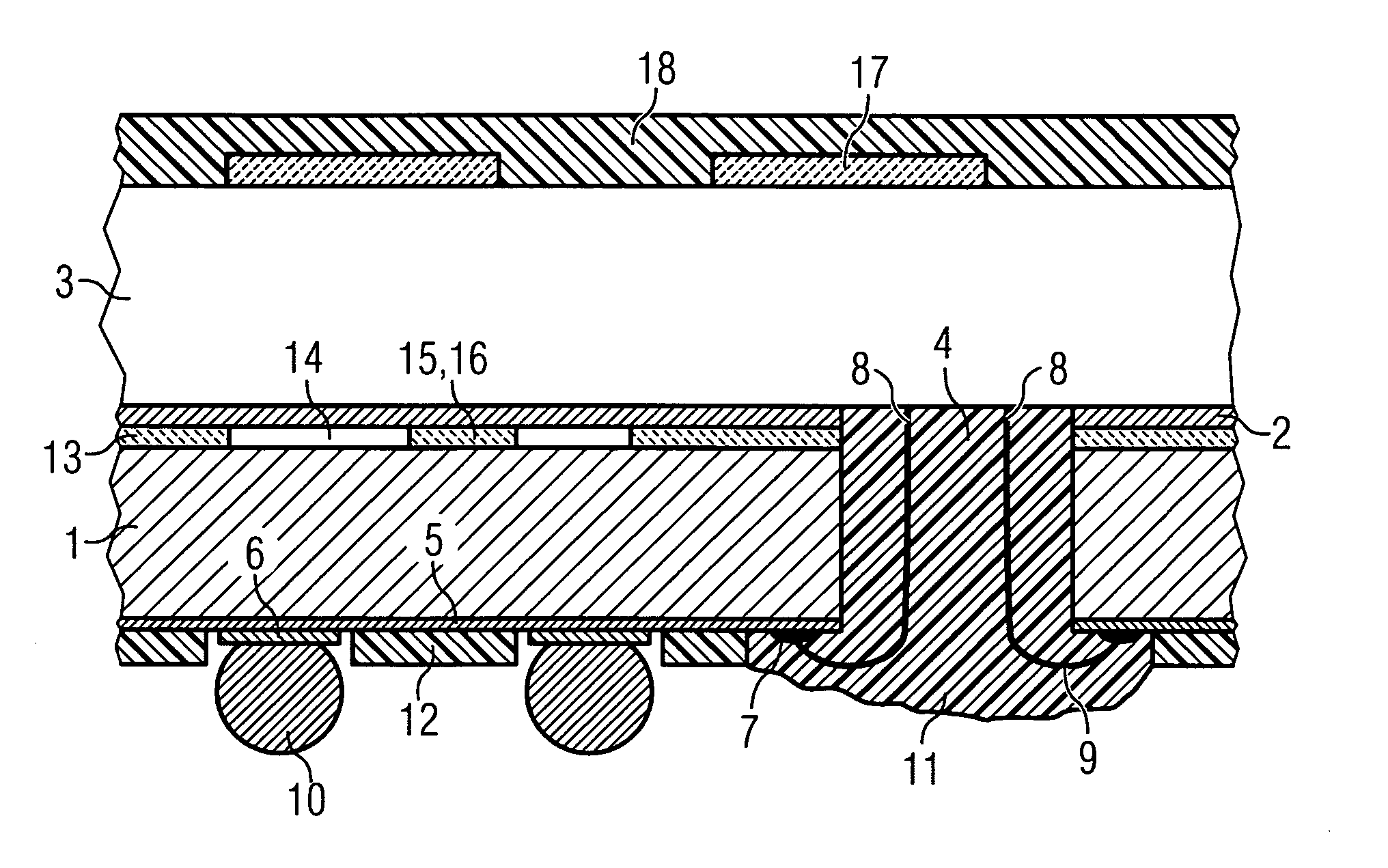
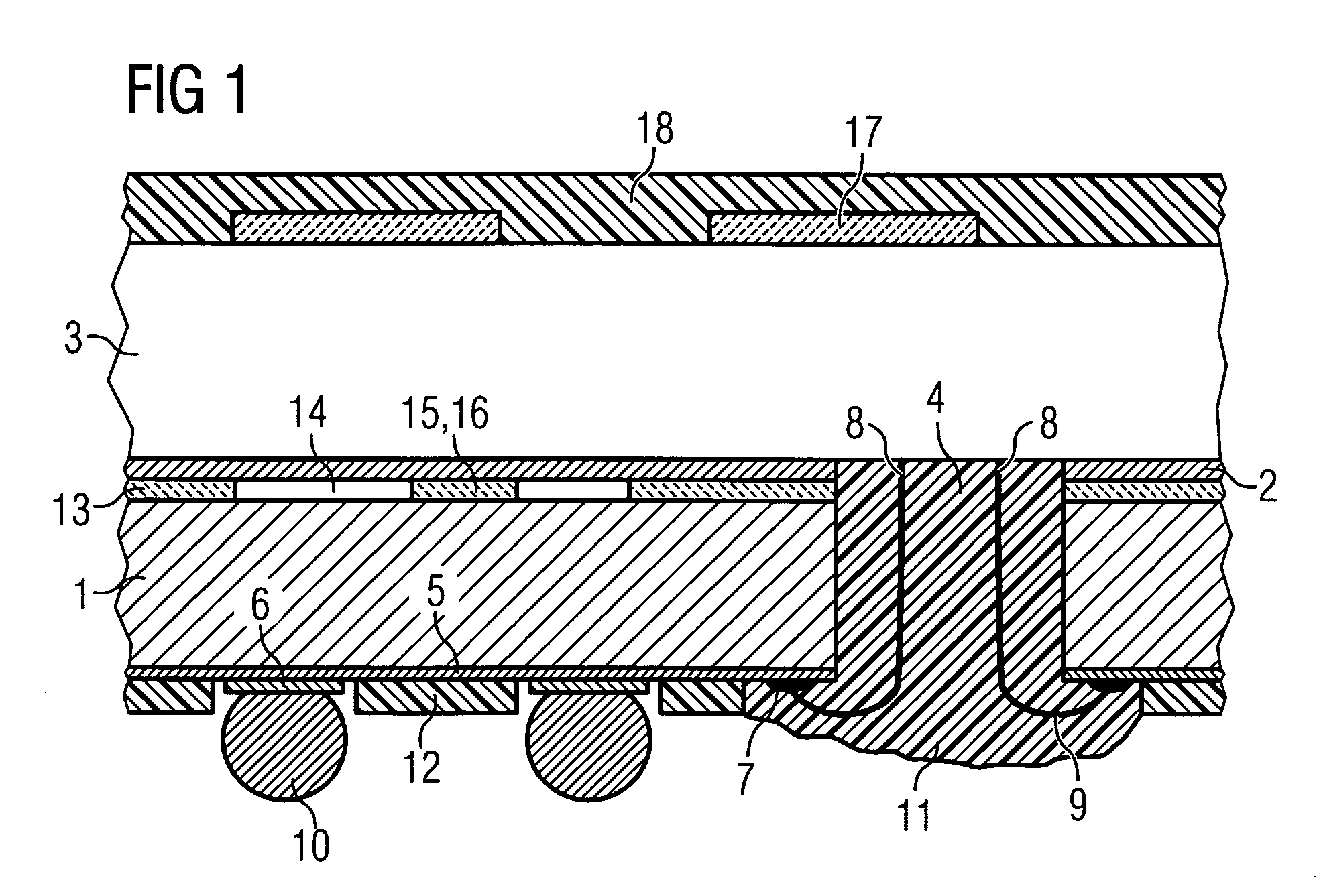
[0056] The sectional representation in FIG. 1 shows a substrate 1, on which a chip 3 is adhesively attached face-down by means of a tape 2. The substrate 1 has a passage, the bonding channel 4, and on the underside a patterned metallization 5. The metallization 5 comprises contact pads 6 arranged in the manner of a grid and bonding pads 7 present in the edge region of the bonding channel 4, and electrically connects them to one another. The double-rowed central contacts 8 of the chip 3 are contacted through the bonding channel 4 by means of wire bridges 9 on the bonding pads 7 and the package is contacted by means of the solder balls 10 present on the contact pads 6 on a module that is not represented. The bonding channel 4 including the wire bridges 9 and the bonding pads 7 is sealed by an encapsulation 11.
[0057] To protect the underside metallization 5 and limit the solder flow during the soldering process for mounting the package on the module that is not represented, the metall...
PUM
 Abstract
Description
Claims
Application Information