

Method of exposure error adjustment in photolithography for multiple products
- Summary
- Abstract
- Description
- Claims
- Application Information
AI Technical Summary
Benefits of technology
Problems solved by technology
Method used
Image

Examples
embodiment
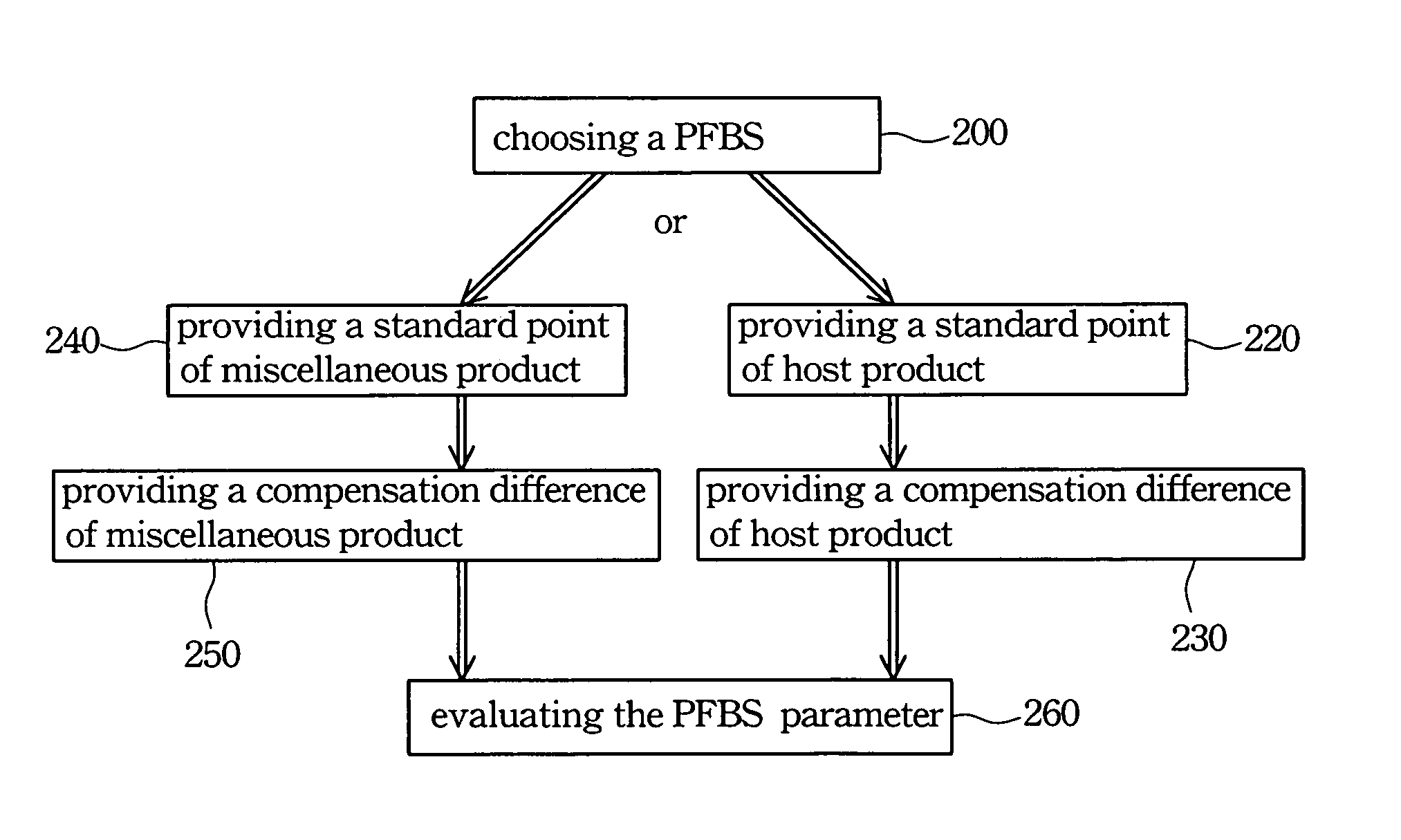
[0026] It is assumed that the host product is mainly processed in s multiple products manufacturing processes, and various minor products are added into operations alternately. The various minor products are generally called the miscellaneous products, and amount of miscellaneous product processed is much smaller than host product.
[0027] Because of the small amount of miscellaneous product processed, the influence of the miscellaneous product on whole product operation is limited, and therefore the host product is not apparently affected by miscellaneous product. Thus, the host product utilizes formula (1) for PFBS parameter calculation to evaluate the PFBS parameter as a exposure adjustment value directly. Referring to FIG. 2, a step 200 for choosing a suitable PFBS is performed first. The PFBS suited to the host product is chosen, and formula (1) is used to calculate the PFBS parameter for the host product. Formula (1) is given as:
PPshost,N=PPshost,N−1−g*B*(PPmhost,N−1−Target) ...
PUM
 Abstract
Description
Claims
Application Information