Transverse or longitudinal patterned synthetic exchange biasing for stabilizing GMR sensors
a synthetic exchange biasing and gmr sensor technology, applied in nanoinformatics, instruments, record information storage, etc., can solve the problems of direct exchange biasing and reduce the sensitivity of the sensor, and achieve the effect of narrow effective magnetic track width, reduced undesirable side readings, and easy fabrication
- Summary
- Abstract
- Description
- Claims
- Application Information
AI Technical Summary
Benefits of technology
Problems solved by technology
Method used
Image
Examples
first preferred embodiment
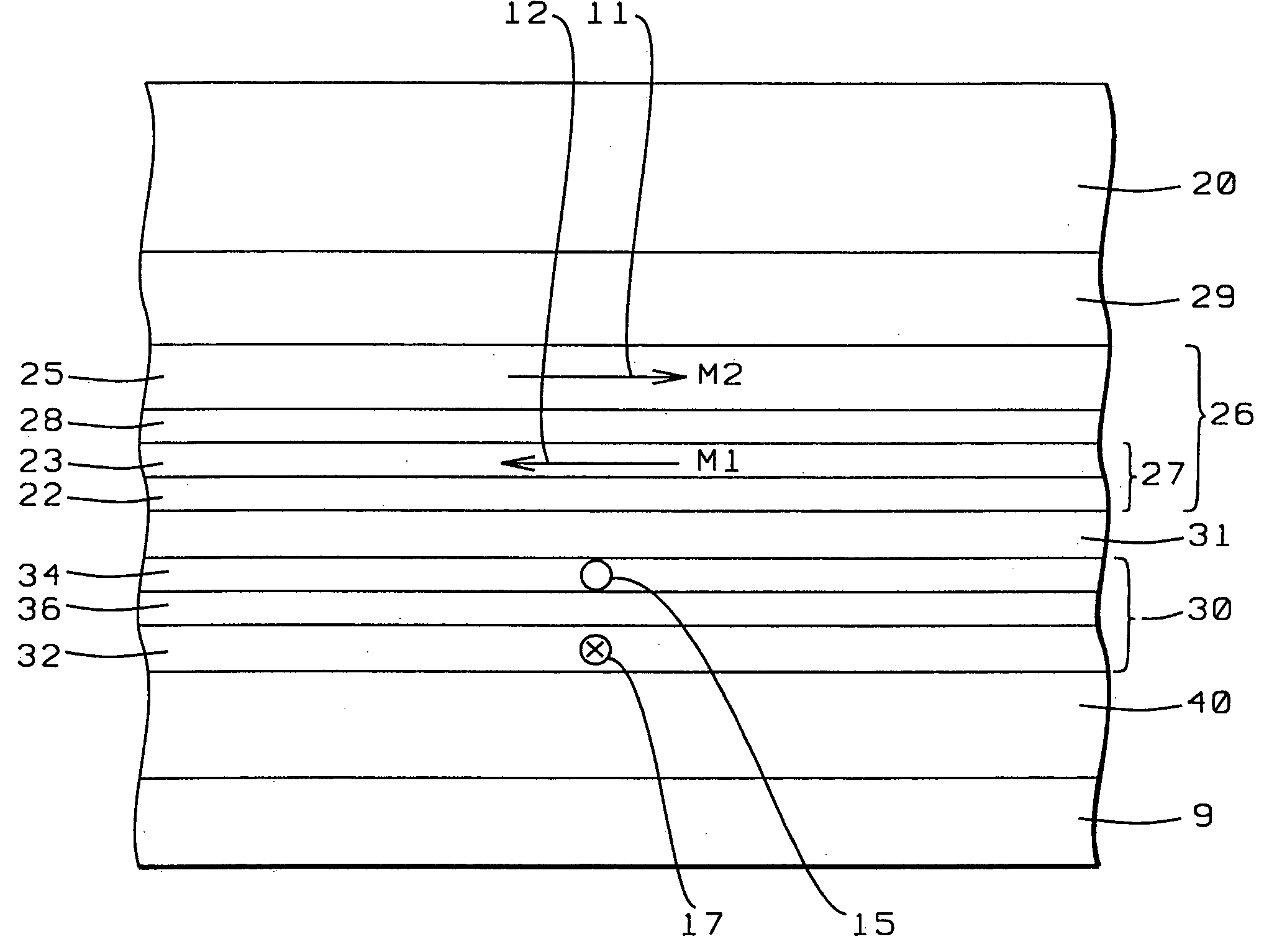
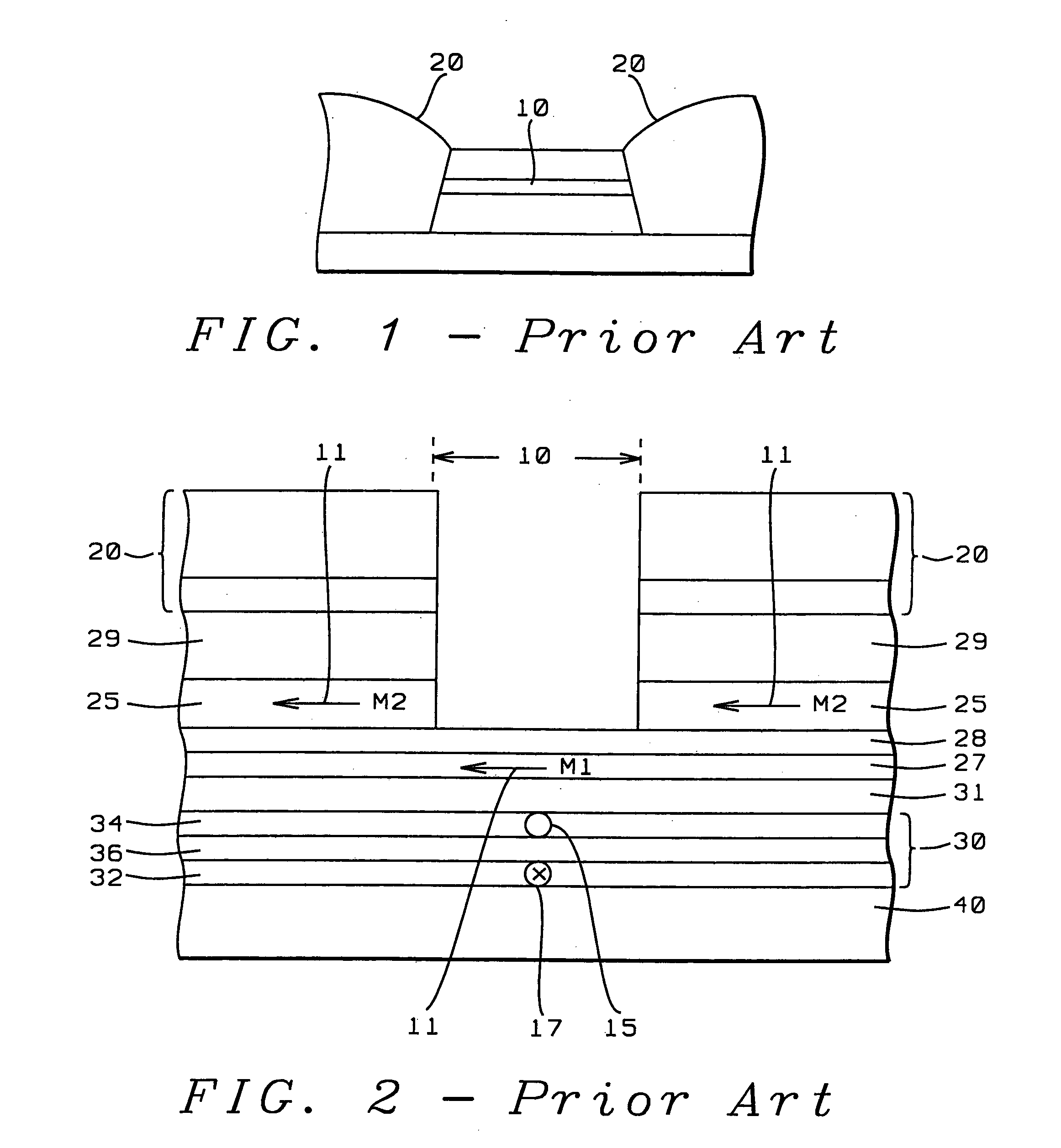
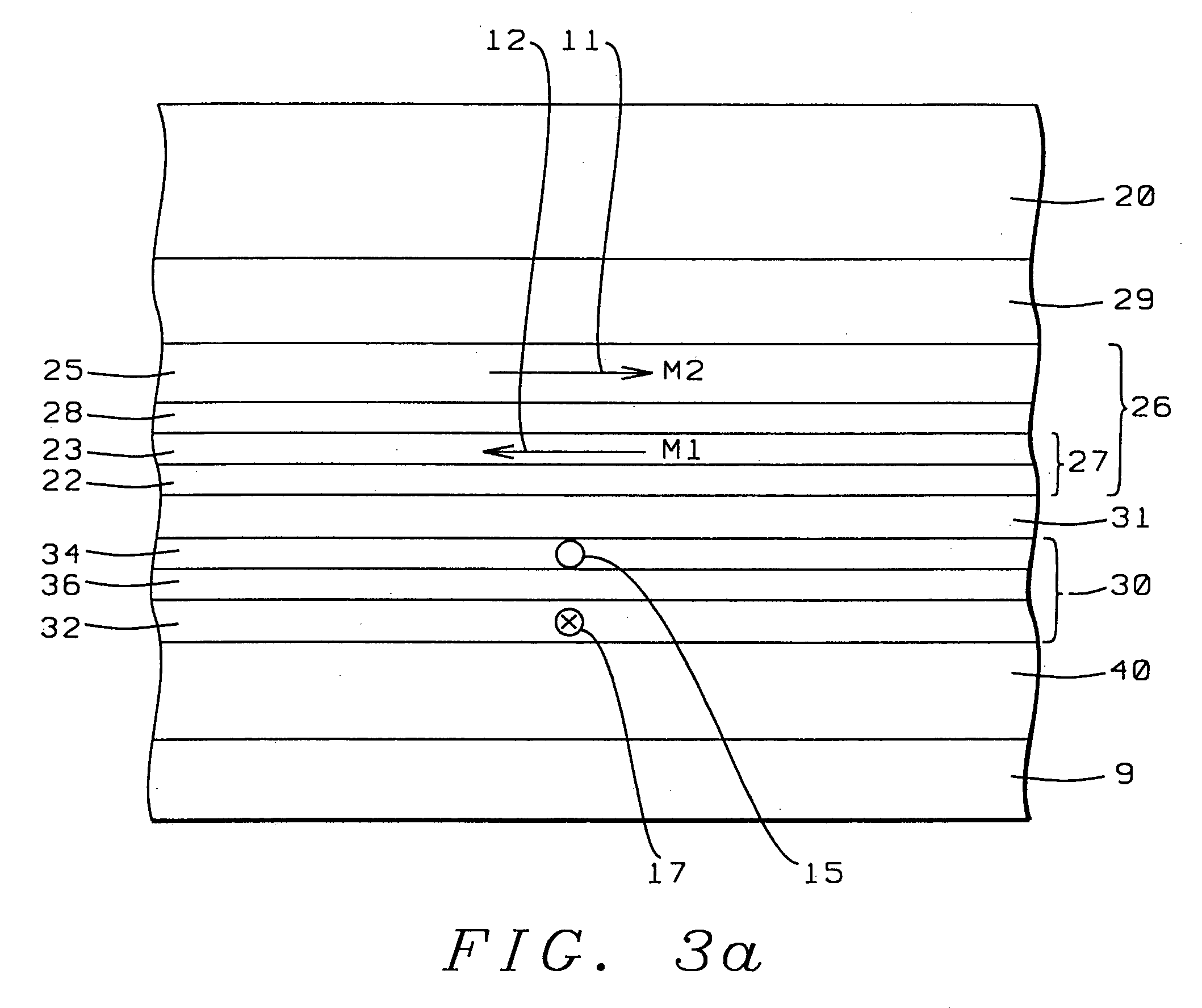
[0031] Referring next to FIG. 3a, there is shown a schematic cross-sectional view of the air bearing surface (ABS) of a synthetic exchange longitudinally biased GMR sensor, before patterning, fabricated in accord with the objects of a first embodiment of the present invention and having the properties and advantages of said embodiment. The device is fabricated in a sequence of three major steps: 1) depositing the sensor layers; 2) annealing and magnetizing the synthetic pinned layer and the synthetic biased free layer; 3) patterning.
[0032] First there is deposited a seed layer (9), which is typically a layer of NiCr deposited to a thickness of between approximately 55 and 65 angstroms with 60 angstroms being preferred. On this seed layer is then deposited a first antiferromagnetic layer (40) to serve as a pinning layer. Typically this pinning layer is a layer of MnPt deposited to a thickness of between approximately 80 and 150 angstroms with 100 angstroms bei...
second preferred embodiment
[0035] Referring next to FIG. 4a, there is shown a schematic cross-sectional view of the air bearing surface (ABS) of a synthetic exchange transversely biased GMR sensor, before patterning, fabricated in accord with the objects of a second embodiment of the present invention and having the properties and advantages of said embodiment. The device is fabricated in a sequence of three major steps: 1) depositing the sensor layers; 2) annealing and magnetizing the synthetic pinned layer and the synthetic biased free layer; 3) patterning.
[0036] First there is deposited a seed layer (9), which is typically a layer of NiCr deposited to a thickness of between approximately 50 and 60 angstroms. On this seed layer is then deposited a first antiferromagnetic layer (40) to serve as a pinning layer. Typically this pinning layer is a layer of MnPt deposited to a thickness of between approximately 100 and 150 angstroms, but other antiferromagnetic materials such as NiMn, PdP...
third preferred embodiment
[0040] Referring next to FIG. 5a, there is shown a schematic cross-sectional view of the air bearing surface (ABS) of a partially fabricated synthetic exchange transversely biased GMR sensor, before the antiparallel magnetization of its biasing layer and before deposition of a conducting lead layer and final patterning, fabricated in accord with the objects of a third embodiment of the present invention and having the properties and advantages of said embodiment. In this embodiment the transverse magnetizations of the pinning layer and free layer are antiparallel to each other at the opposite ends of the sensor where they are beneath the conducting lead layers. This configuration has been shown to have two advantages: 1) prevention of the bias point shift at the center active region of the free layer and 2) minimization of side reading at both sides of the sensor element.
[0041] The device is fabricated in a sequence of four steps: 1) depositing the sensor layers up to and including...
PUM
| Property | Measurement | Unit |
|---|---|---|
| thickness | aaaaa | aaaaa |
| thickness | aaaaa | aaaaa |
| thickness | aaaaa | aaaaa |
Abstract
Description
Claims
Application Information


