Method for fabricating a patterned synthetic longitudinal exchange biased GMR sensor

a technology of longitudinal exchange and patterned synthetics, applied in nanoinformatics, instruments, record information storage, etc., can solve the problems of direct exchange biasing and reduce the sensitivity of the sensor, and achieve the effects of stabilizing the bias point of the free layer, reducing signal contributions, and high pinning fields

Inactive Publication Date: 2005-02-22
HEADWAY TECH INC
View PDF7 Cites 33 Cited by
  • Summary
  • Abstract
  • Description
  • Claims
  • Application Information

AI Technical Summary

Benefits of technology

The NiCr is a seed layer, AFM denotes an antiferromagnetic pinning layer for the bottom synthetic pinned layer of CoFe (AP2)/Ru/CoFe(AP1), wherein the two ferromagnetic exchange coupled CoFe layers are labeled AP1 & AP2 to distinguish them. The Cu layer is a conducting, non-magnetic spacer layer separating the synthetic pinned layer from the CoFe—NiFe ferromagnetic free layer (a bilayer). This latter bilayer is antiferromagnetically exchange coupled across a Ru layer to a (patterned) CoFe biasing layer, forming the synthetic exchange coupled bias structure. The exchange biased layer is itself antiferromagnetically pinned by direct exchange coupling with an antiferromagnetic layer, again denoted AFM, over which is a conductive lead layer of Ta/Au. In contrast to the structural form of the first embodiment, the same antiferromagnetic material, typically either IrMn or MnPt, can serve in both locations designated AFM. An important advantage of the transverse biasing is that the magnetic field of the free and pinned layers are in the same direction, producing a plateau region under low external field wherein the free layer magnetization and the pinned layer magnetizations do not rotate relative to each other. This is particularly important for reducing signal contributions from ...

Problems solved by technology

For trackwidths less than 0.2 microns (μm), the traditional abutted junction hard bias structure discussed above becomes unsuitable because the strong magnetostatic coupling at the junction surface actually pins the magnetization of the (very narrow) biased layer (the free layer), making it les...

Method used


Image

  • Method for fabricating a patterned synthetic longitudinal exchange biased GMR sensor
  • Method for fabricating a patterned synthetic longitudinal exchange biased GMR sensor
  • Method for fabricating a patterned synthetic longitudinal exchange biased GMR sensor

Examples


first preferred embodiment

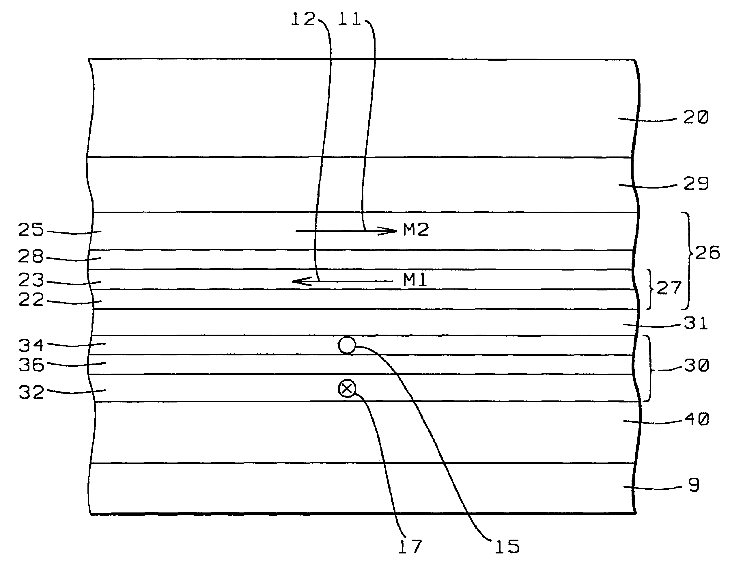
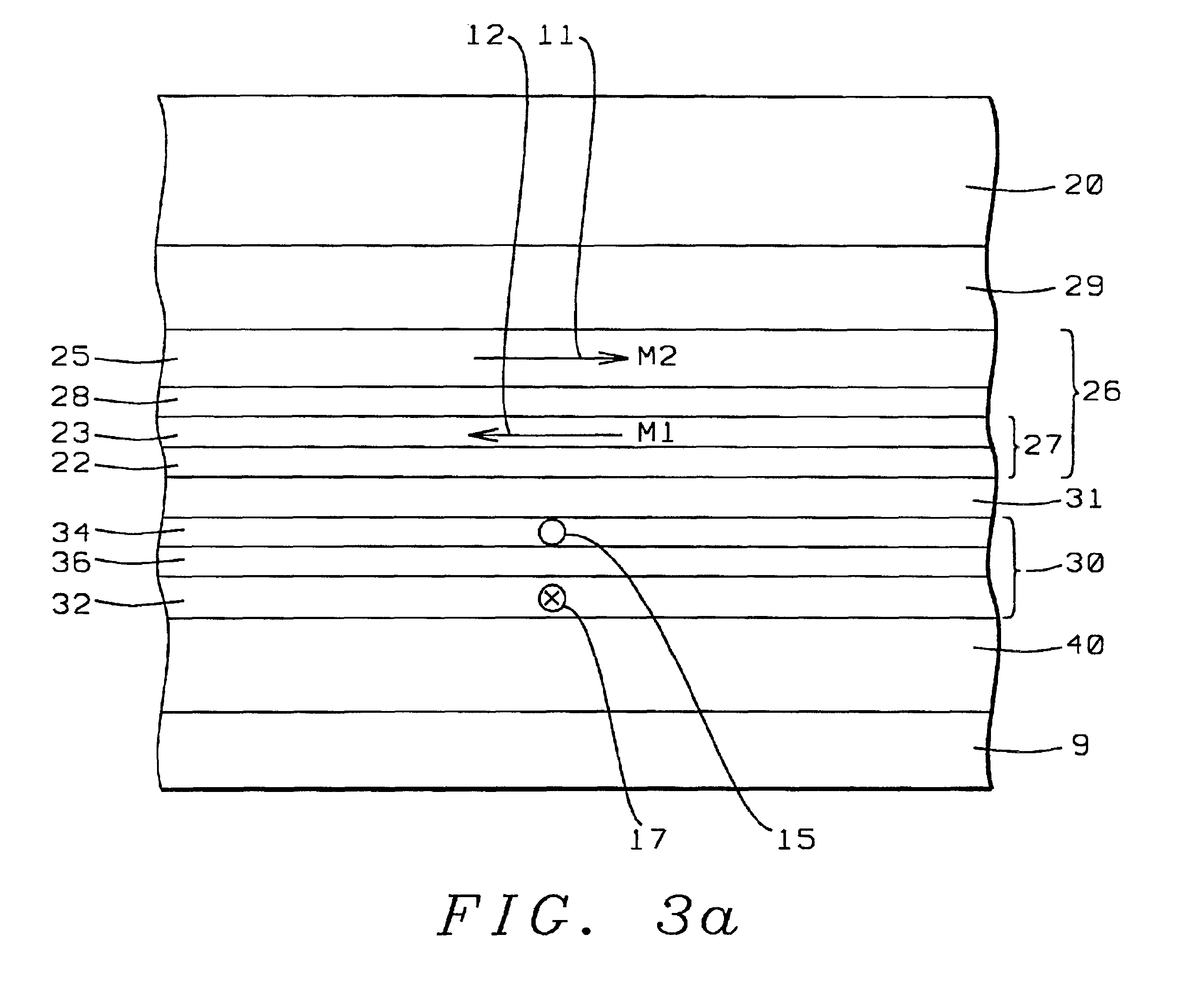
Referring next to FIG. 3a, there is shown a schematic cross-sectional view of the air bearing surface (ABS) of a synthetic exchange longitudinally biased GMR sensor, before patterning, fabricated in accord with the objects of a first embodiment of the present invention and having the properties and advantages of said embodiment. The device is fabricated in a sequence of three major steps: 1) depositing the sensor layers; 2) annealing and magnetizing the synthetic pinned layer and the synthetic biased free layer; 3) patterning.

1) Deposition Process

First there is deposited a seed layer (9), which is typically a layer of NiCr deposited to a thickness of between approximately 55 and 65 angstroms with 60 angstroms being preferred. On this seed layer is then deposited a first antiferromagnetic layer (40) to serve as a pinning layer. Typically this pinning layer is a layer of MnPt deposited to a thickness of between approximately 80 and 150 angstroms with 100 angstroms being preferred. On ...

second preferred embodiment

Referring next to FIG. 4a, there is shown a schematic cross-sectional view of the air bearing surface (ABS) of a synthetic exchange transversely biased GMR sensor, before patterning, fabricated in accord with the objects of a second embodiment of the present invention and having the properties and advantages of said embodiment. The device is fabricated in a sequence of three major steps: 1) depositing the sensor layers; 2) annealing and magnetizing the synthetic pinned layer and the synthetic biased free layer; 3) patterning.

1) Deposition Process

First there is deposited a seed layer (9), which is typically a layer of NiCr deposited to a thickness of between approximately 50 and 60 angstroms. On this seed layer is then deposited a first antiferromagnetic layer (40) to serve as a pinning layer. Typically this pinning layer is a layer of MnPt deposited to a thickness of between approximately 100 and 150 angstroms, but other anti ferromagnetic materials such as NiMn, PdPtMn, FeMn or IrM...

third preferred embodiment

Referring next to FIG. 5a, there is shown a schematic cross-sectional view of the air bearing surface (ABS) of a partially fabricated synthetic exchange transversely biased GMR sensor, before the antiparallel magnetization of its biasing layer and before deposition of a conducting lead layer and final patterning, fabricated in accord with the objects of a third embodiment of the present invention and having the properties and advantages of said embodiment. In this embodiment the transverse magnetizations of the pinning layer and free layer are antiparallel to each other at the opposite ends of the sensor where they are beneath the conducting lead layers. This configuration has been shown to have two advantages: 1) prevention of the bias point shift at the center active region of the free layer and 2) minimization of side reading at both sides of the sensor element.

The device is fabricated in a sequence of four steps: 1) depositing the sensor layers up to and including the exchange b...


PUM

PropertyMeasurementUnit
Temperatureaaaaaaaaaa
Timeaaaaaaaaaa

Abstract

Patterned, longitudinally and transversely antiferromagnetically exchange biased GMR sensors are provided which have narrow effective trackwidths and reduced side reading. The exchange biasing significantly reduces signals produced by the portion of the ferromagnetic free layer that is underneath the conducting leads while still providing a strong pinning field to maintain sensor stability. In the case of the transversely biased sensor, the magnetization of the free and biasing layers in the same direction as the pinned layer simplifies the fabrication process and permits the formation of thinner leads by eliminating the necessity for current shunting.

Description

BACKGROUND OF THE INVENTION1. Field of the InventionThis invention relates generally to the fabrication of a giant magnetoresistive (GMR) magnetic field sensor for a magnetic read head, more specifically to the use of either transverse or longitudinal synthetic exchange biasing to stabilize, suppress side reading and reduce the magnetic track width (MRW) of such a sensor.2. Description of the Related ArtMagnetic read heads whose sensors make use of the giant magnetoresistive effect (GMR) in the spin-valve configuration (SVMR) base their operation on the fact that magnetic fields produced by data stored in the medium being read cause the direction of the magnetization of one layer in the sensor (the free magnetic layer) to move relative to a fixed magnetization direction of another layer of the sensor (the fixed or pinned magnetic layer). Because the resistance of the sensor element is proportional to the cosine of the (varying) angle between these two magnetizations, a constant curr...

Claims


Application Information

Patent Timeline
IPC IPC(8): G01R33/06G01R33/09G11B5/39G11B5/31
CPCB82Y10/00B82Y25/00G01R33/093G11B5/3143G11B5/3163G11B5/3932Y10T29/49032Y10T29/49052Y10T29/49044Y10T29/49048Y10T29/49034Y10T29/49046G11B2005/3996
Inventor HORNG, CHENG T.LI, MINTONG, RU-YINGLI, YUN-FEIZHENG, YOU FENGLIAO, SIMONJU, KOCHANHAN, CHERNG CHYI
Owner HEADWAY TECH INC
Why Eureka
Try Eureka