Method for fabricating silicide

Active Publication Date: 2005-06-09
UNITED MICROELECTRONICS CORP
View PDF6 Cites 13 Cited by
  • Summary
  • Abstract
  • Description
  • Claims
  • Application Information

AI Technical Summary

Benefits of technology

[0008] A processing method for fabricating silicide is provided. First of all, a semiconductor structure having a semiconductor surface and an insulation surface is provided. Next, an epitaxial layer on the semiconductor surface is formed. And, the semiconductor structure is treated. The treating step is that the removal rate of

Problems solved by technology

In view of the prior art, there are many disa

Method used


Image

  • Method for fabricating silicide
  • Method for fabricating silicide
  • Method for fabricating silicide

Examples


Embodiment Construction

[0012] Some sample embodiments of the invention will now be described in greater detail. Nevertheless, it should be recognized that the present invention could be practiced in a wide range of others.

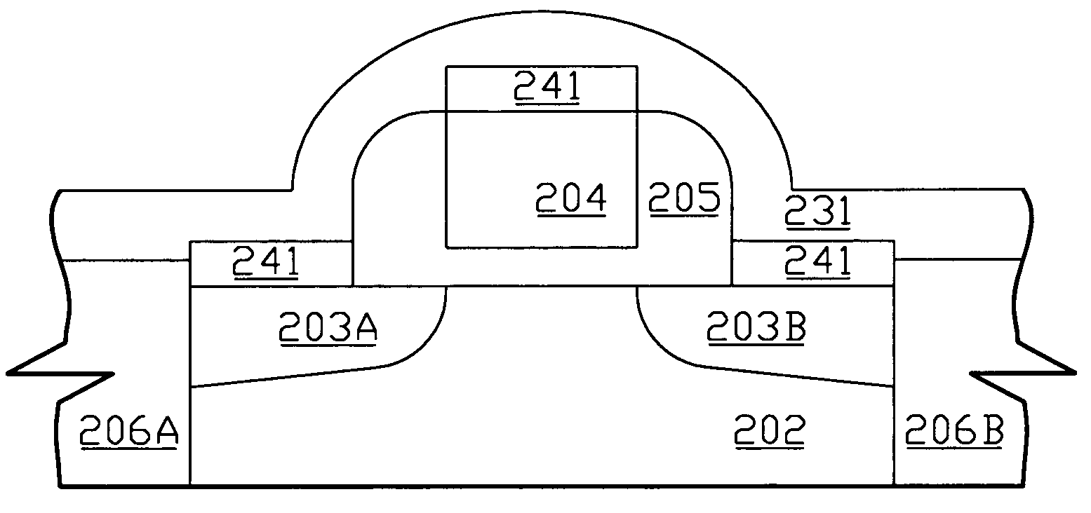
[0013] A processing method for fabricating silicide is provided. First of all, a semiconductor structure having a semiconductor surface and an insulation surface is provided. Next, an epitaxial layer on the semiconductor surface is formed. And, the semiconductor structure is treated. The treating step is that the removal rate of the insulation surface is faster than the removal rate of the epitaxial layer. Then, a metal layer on the epitaxial layer is formed. Finally, heating the epitaxial layer forms silicide. The treating step prevents the insulation surface from the formation of the silicide so as to reduce the degradation of the device characteristics.

[0014] One embodiment of this invention is shown in FIGS. 2A to 2E. FIG. 2A shows the basic semiconductor structure 201 implemented ...


PUM


Abstract

A processing method for fabricating silicide is provided. First of all, a semiconductor structure having a semiconductor surface and an insulation surface is provided. Next, an epitaxial layer on the semiconductor surface is formed. And, the semiconductor structure is treated. The treat step is that the removal rate of the insulation surface is faster than the removal rate of the epitaxial layer. Then, a metal layer on the epitaxial layer is formed. Finally, heating the epitaxial layer forms silicide. The treatment step prevents the insulation surface from the formation of the silicide so as to reduce the degradation of device characteristics.

Description

BACKGROUND OF THE INVENTION [0001] 1. Field of the Invention [0002] The present invention generally relates to the semiconductor fabrication process, and more particularly to a method for fabricating silicide. [0003] 2. Description of the Prior Art [0004] As the semiconductor processing dimensions are scaled down, the parasitic resistance such as contact and sheet resistance increases. To reduce such parasitic resistance, the silicide process attracted much attention. Among various suicides, cobalt silicide (CoSi2) and titanium silicide (TiSi2) are the most attractive and studied. They can be applied to the SALIDE (self-aligned silicide) process and show the lowest resistivity among the various silicides. For the improvement of thermal stability, epitaxially grown silicide films are required. [0005] The prior art fabrication sequence is shown in FIG. 1A to 1D. FIG. 1A shows the basic semiconductor structure 101, which comprises a substrate 102 with two doped regions 103A, 103B, a ga...

Claims


Application Information

Patent Timeline
IPC IPC(8): H01L21/285H01L21/3205H01L21/336H01L21/44H01L29/78
CPCH01L21/28518H01L29/41783H01L29/78H01L29/66628H01L29/665
Inventor WU, BING-CHANG
Owner UNITED MICROELECTRONICS CORP
Why Eureka
Try Eureka