High-frequency power supply structure and plasma cvd device using the same

a power supply structure and high-frequency technology, applied in the direction of coatings, electric discharge lamps, electric lighting sources, etc., can solve the problems of less uniform power in the plane formed by the electrode and increase the uniformity of the plasma, so as to increase the ratio of the power inputted into the space between the electrode and the substrate to the radio frequency power transmitted from an rf power sour

Inactive Publication Date: 2005-06-16
MITSUBISHI HEAVY IND LTD
View PDF22 Cites 4 Cited by
  • Summary
  • Abstract
  • Description
  • Claims
  • Application Information

AI Technical Summary

Benefits of technology

[0034] According to the present eighth means, the plasma CVD device can exhibit the function of any one of the first to the seventh means. Thus, the ratio of the power inputted into the space between the electrode and the substrate to the radio frequency power transmitted from an RF power source can be increased. Also, a stable radio frequency power can be supplied into the space between the electrode and the substrate and a generation of a uniform plasma distribution in a wide area becomes possible.

Problems solved by technology

Thereby, even in the case where the electrode is constructed having plural connecting portions, the imbalances of the incident power between each of the plural connecting portions hardly occur so that a non-uniformity of the power in the plane formed by the electrode becomes less and a uniformity of the plasma increases.

Method used


Image

  • High-frequency power supply structure and plasma cvd device using the same
  • High-frequency power supply structure and plasma cvd device using the same
  • High-frequency power supply structure and plasma cvd device using the same

Examples


Embodiment Construction

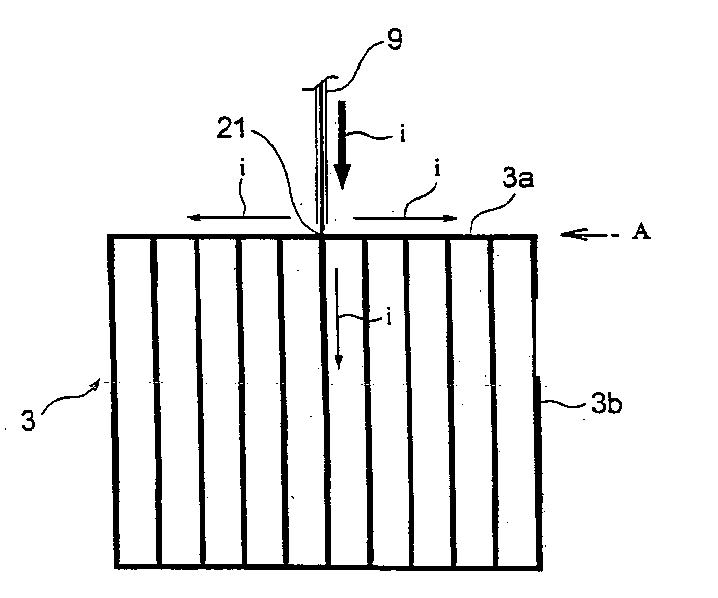
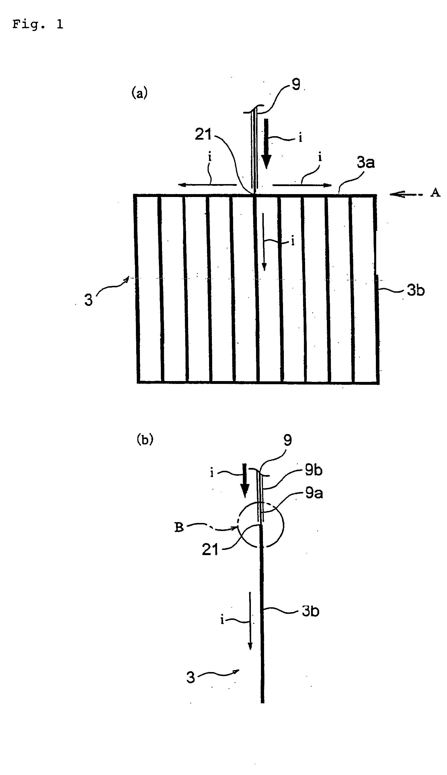
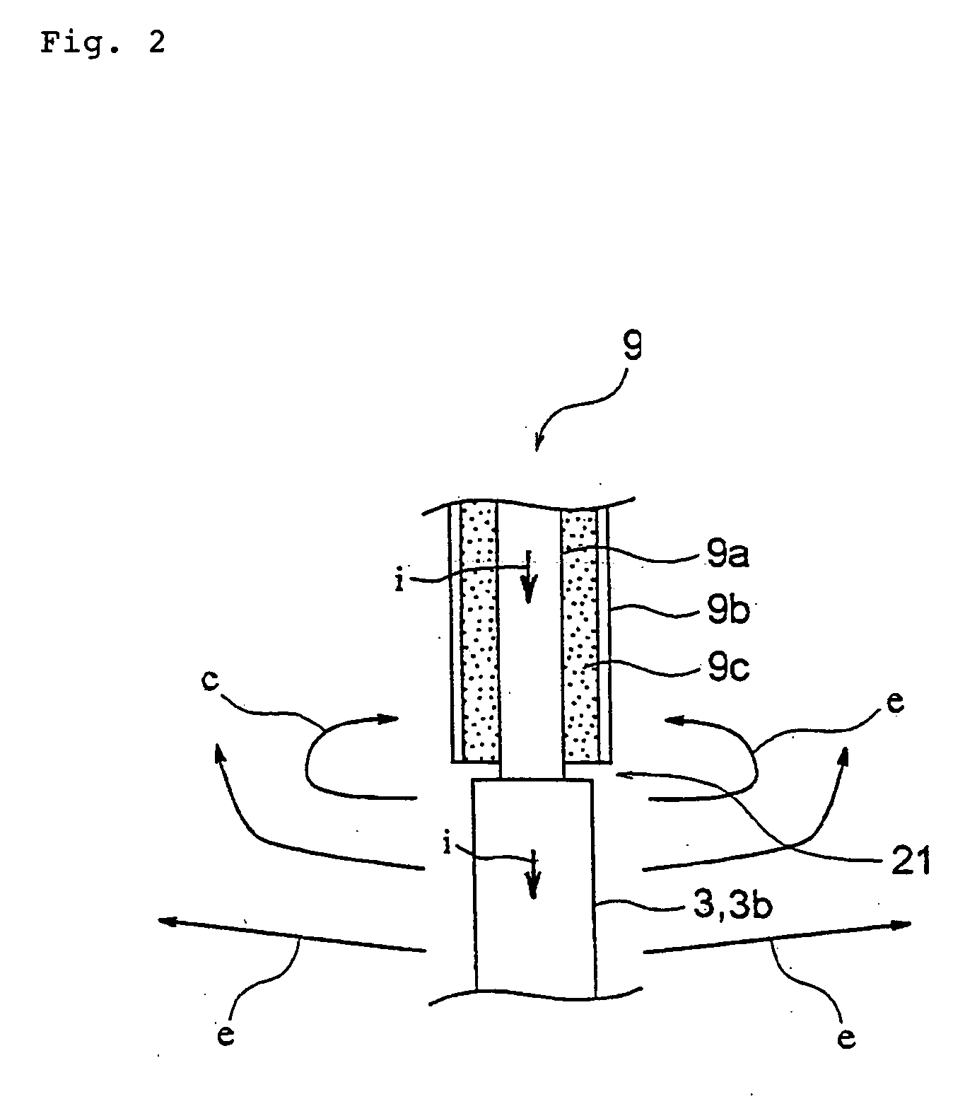
[0041] A radio frequency power supply structure and a plasma CVD device comprising the same of one embodiment according to the present invention will be described with reference to FIGS. 1 to 3.

[0042]FIG. 1 comprises FIGS. 1(a) and 1(b), wherein FIG. 1(a) is a front view of a ladder electrode and an RF cable of the radio frequency power supply structure of the present embodiment and FIG. 1(b) is a side view seen in the direction of arrow A of FIG. 1(a). FIG. 2 is an enlarged cross sectional view of a connecting portion shown as portion B of FIG. 1(b). FIG. 3 comprises FIGS. 3(a) and 3(b) both being the same enlarged cross sectional views as FIG. 2 showing variations of the connecting portion. It is to be noted that an entire construction of the plasma CVD device comprising the radio frequency power supply structure of the present embodiment is the same as that shown in FIG. 4 and an illustration thereof is omitted.

[0043] As seen in FIGS. 1(a) and 1(b), except the structure of the ...


PUM

PropertyMeasurementUnit
radio frequency poweraaaaaaaaaa
right angleaaaaaaaaaa
frequencyaaaaaaaaaa

Abstract

A radio frequency power supply structure and a plasma CVD device comprising the same are provided in which reflection of radio frequency power at a connecting portion where an RF cable connects to an electrode is reduced so that incidence of the radio frequency power into the electrode increases. In the radio frequency power supply structure for use in a device generating plasma by charging a plate-like electrode with a radio frequency power, the radio frequency power supply structure supplying the electrode with the radio frequency power from an RF cable, the RF cable is positioned on an extended plane of a plane formed by the electrode to connect to the electrode at a connecting portion provided on an end peripheral portion of the electrode. The RF cable connects to the electrode substantially in the same plane as the plane formed by the electrode. Voltage acting after the connecting portion becomes symmetric relative to the plane formed by the electrode and the electric line of force also becomes symmetric. Thereby, change of impedance at the connecting portion is reduced, reflection of the radio frequency power at the connecting portion is reduced, incidence of the radio frequency power into the electrode increases and the efficiency of film forming and surface treatment is enhanced.

Description

TECHNICAL FIELD [0001] The present invention relates to a radio frequency power supply structure and a plasma CVD (chemical vapor deposition) device comprising the same for use in a device or system generating plasma by charging a plate-like electrode with a radio frequency power. This radio frequency power supply structure is able to efficiently supply the electrode with the radio frequency power from an RF cable (radio frequency power cable). BACKGROUND ART [0002] As a general example of a prior art device generating plasma by charging a plate-like electrode with a radio frequency power, a construction of a plasma CVD device generating plasma to form a silicon film or the like on a target substrate will be described with reference to FIG. 4. Also, a radio frequency power supply structure supplying this electrode with the radio frequency power from an RF cable will be described with reference to FIGS. 5 and 6. FIG. 4 is a schematic constructional view showing one example of a prior...

Claims


Application Information

Patent Timeline
Patent Type & Authority Applications(United States)
IPC IPC(8): C23C16/509H01J37/32H01L21/205
CPCH01J37/32577H01J37/32082
Inventor MASHIMA, HIROSHIKAWAMURA, KEISUKETAKANO, AKEMITAKEUCHI, YOSHIAKISHIGEMIZU, TETSUROAOI, TATSUFUMI
Owner MITSUBISHI HEAVY IND LTD
Why Eureka
Try Eureka