Inductive coupling source

A technology of inductive coupling and inductively coupled coils, which is applied in the field of microelectronics, can solve problems such as excessive inductance, increased inhomogeneity of radial plasma density, and unstable impedance matching, so as to achieve uniform magnetic field strength, reduce dependence, The effect of superior performance

Active Publication Date: 2010-05-12
BEIJING NAURA MICROELECTRONICS EQUIP CO LTD
View PDF5 Cites 0 Cited by
  • Summary
  • Abstract
  • Description
  • Claims
  • Application Information

AI Technical Summary

Problems solved by technology

In this case, the problem faced by the traditional planar spiral coil is that the inductance is too large, and the corresponding radial plasma density non-uniformity will also increase.
Because the large inductance causes large voltage and unstable impedance matching between the coil terminals, the large voltage also causes capacitive coupling between the coil and the plasma, resulting in low coupling efficiency and uneven plasma distribution
Therefore, most of the current etching equipment is facing the problem of uneven etching rate, which has caused great limitations to the semiconductor manufacturing process.

Method used


Image

  • Inductive coupling source
  • Inductive coupling source
  • Inductive coupling source

Examples


Embodiment Construction

[0027] The specific implementation manner of the inductive coupling source of the present invention will be further described in detail below in conjunction with the accompanying drawings, but it is not used to limit the protection scope of the present invention.

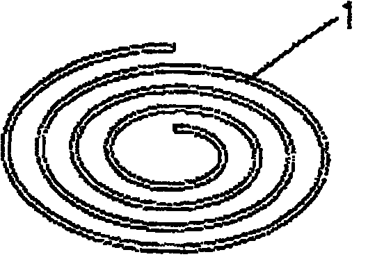
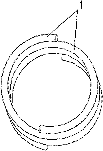
[0028] see Figure 2 to Figure 4 . The structure of the first embodiment of the inductively coupled source of the present invention includes a pair of inductively coupled coils 1 and excitation sources that are nested and arranged in complete symmetry. The inductively coupled coil is an involute multi-turn three-dimensional coil. The excitation source is a radio frequency power source.

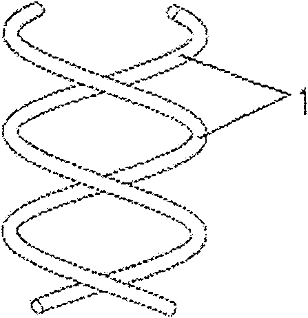
[0029] see Figure 5 . The structure of the second embodiment of the inductively coupled source of the present invention includes an inner group coil 2 and an outer group coil 3 and an excitation source connected in series or in parallel, wherein the inner group coil 2 and the outer group coil 3 are each composed of a pair of co...


PUM

PropertyMeasurementUnit
sizeaaaaaaaaaa

Abstract

The invention relates to microelectronics technology. The invention includes inductively coupled source inductance coupling coil, coil inductance coupling is a linear three-dimensional multi-coil turns. Inductively Coupled coil symmetrical layout of a number of nested right, with the series divided into the within the coil groups and the outer coil group. The strengths and positive effect of the source inductance coupling invention is: the invention, fully three-dimensional symmetric coil structure is designed for electromagnetic fields in the reaction chamber of the internal distribution of symmetry, thereby improving the response of the plasma within the chamber evenly distributed, make the chip surface at various points of the etching rate closer. The invention of the technology programs can be well controlled from the chip to the edge of the central etching rate and uniformity even with the increasing size of the chip.

Description

technical field [0001] The invention relates to the technical field of microelectronics, in particular to an inductive coupling source used in the manufacturing process of manufacturing integrated circuits (IC) or MEMS devices. Background technique [0002] Plasma devices are widely used in fabrication processes for fabricating integrated circuits (ICs) or MEMS devices. Among them, inductively coupled plasma (ICP) is widely used in etching and other processes. Under low pressure, the reactive gas is excited by radio frequency power to generate ionization to form a plasma. The plasma contains a large number of active particles such as electrons, ions, excited atoms, molecules and free radicals. These active reactive groups and the engraved Various physical and chemical reactions occur on the surface of the corrosive material and form volatile products, thereby changing the surface properties of the material. [0003] In semiconductor processing, the process gas entering the...

Claims


Application Information

Patent Timeline
Patent Type & Authority Patents(China)
IPC IPC(8): H05H1/24H01F5/00H01F38/14
Inventor 宋巧丽胡谦
Owner BEIJING NAURA MICROELECTRONICS EQUIP CO LTD
Why Eureka
Try Eureka