Methods of forming spin-on-glass insulating layers in semiconductor devices and associated semiconductor device

Inactive Publication Date: 2005-06-16
SAMSUNG ELECTRONICS CO LTD
View PDF6 Cites 21 Cited by
  • Summary
  • Abstract
  • Description
  • Claims
  • Application Information

AI Technical Summary

Benefits of technology

[0012] In these methods, sufficient heat treatment may be provided to the semiconductor structure to convert the spin-on-glass layer into a silicon oxide layer. The metal oxide layer may be formed using an atomic layer deposition process. The metal oxide layer may be formed by forming a metal layer on the semiconductor structure and thereafter oxidizing the metal layer. In spe

Problems solved by technology

As this aspect ratio increases, it may become more difficult to satisfactorily fill the gap in subsequent steps of the manufacturing process.
However, the high temperature applied to the device during the reflow process may cause thermal damage to the substrate.
However, the TEOS or the USG may have a strong tendency to form a void or seam during the deposition process, and thus may not fully fill the gaps in the fine pattern.
However, when the SOG layer is formed on a pattern that has very fine gaps, it may be difficult to supply adequate oxygen adjacent the botto

Method used


Image

  • Methods of forming spin-on-glass insulating layers in semiconductor devices and associated semiconductor device
  • Methods of forming spin-on-glass insulating layers in semiconductor devices and associated semiconductor device
  • Methods of forming spin-on-glass insulating layers in semiconductor devices and associated semiconductor device

Examples


Example

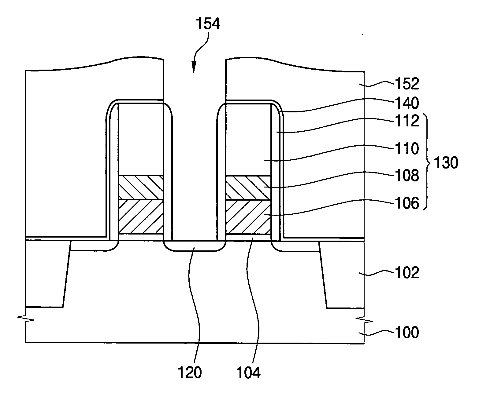
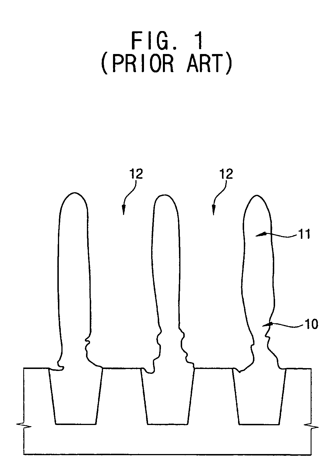
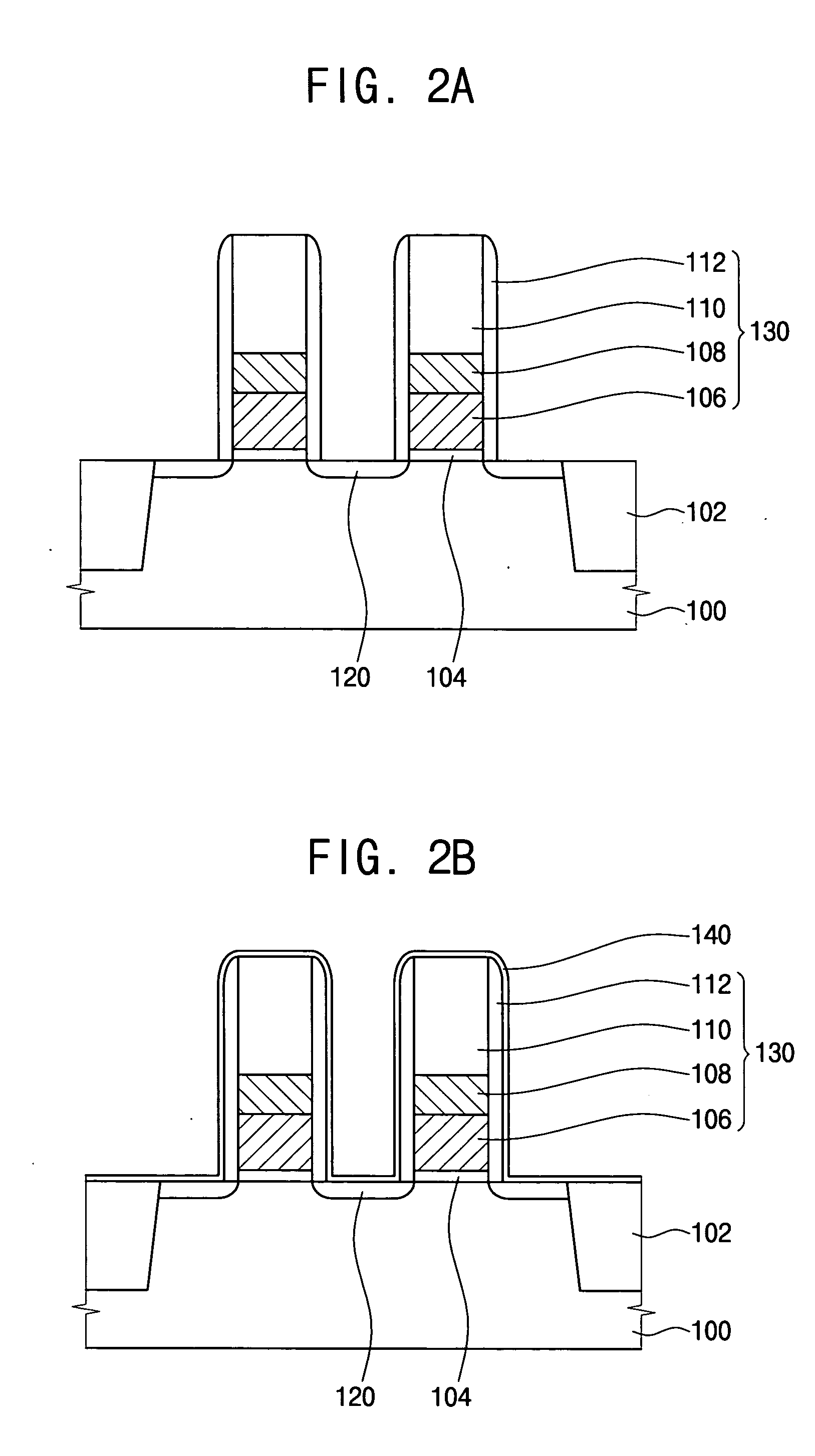
[0027] Embodiments of the present invention now will be described more fully hereinafter with reference to the accompanying drawings, in which embodiments of the invention are shown. This invention may, however, be embodied in many different forms and should not be construed as limited to the embodiments set forth herein. Rather, these embodiments are provided so that this disclosure will be thorough and complete, and will fully convey the scope of the invention to those skilled in the art. Like numbers refer to like elements throughout.

[0028] It will be understood that, although the terms first, second, etc. may be used herein to describe various elements, these elements should not be limited by these terms. These terms are only used to distinguish one element from another. For example, a first element could be termed a second element, and, similarly, a second element could be termed a first element, without departing from the scope of the present invention. As used herein, the te...


PUM


Abstract

Methods of forming an insulating layer in a semiconductor device are provided in which a metal oxide layer is formed on a semiconductor structure that includes a plurality of gap regions thereon. A spin-on-glass layer is formed on the metal oxide layer, and then the semiconductor structure is heated to a temperature of at least about 400° C. The spin-on-glass layer may comprise a siloxane-based material, a silanol-based material or a silazane-based material.

Description

CROSS-REFERENCE OF RELATED APPLICATIONS [0001] This application claims priority under 35 U.S.C. § 119 from Korean Patent Application No. 2003-89305, filed on Dec. 10, 2003, the disclosure of which is incorporated herein by reference as if set forth in its entirety.FIELD OF THE INVENTION [0002] The present invention relates to methods of manufacturing semiconductor devices and, more particularly, to methods of forming semiconductor device insulating layers and to the semiconductor devices formed by such methods. BACKGROUND OF THE INVENTION [0003] As semiconductor devices become more highly integrated, very fine patterns may be formed on the semiconductor substrate. As part of the fabrication process, gaps or holes are often formed in these very fine patterns such as, for example, the contact holes that may be formed during the manufacture of various semiconductor memory devices. As the size of the pattern is reduced, the aspect ratio of the gaps in the pattern (the ratio of the gap h...

Claims


Application Information

Patent Timeline
IPC IPC(8): H01L21/316H01L21/60H01L21/768H01L21/31
CPCH01L21/316H01L21/76828H01L21/76897H01L21/76837H01L21/76829H01L21/02164H01L21/02175H01L21/02318H01L21/022H01L21/0228H01L21/31
Inventor GOO, JUSEONHONG, EUNKEEKIM, HONG-GUNNA, KYU-TAE
Owner SAMSUNG ELECTRONICS CO LTD
Why Eureka
Try Eureka