Method for making high density nonvolatile memory

Inactive Publication Date: 2005-01-20
SANDISK TECH LLC
View PDF9 Cites 24 Cited by
  • Summary
  • Abstract
  • Description
  • Claims
  • Application Information

AI Technical Summary

Benefits of technology

[0007] Other embodiments provide for improved density and decreased feature size and height of portions of the memory cell. For example, a preferred embodiment provides for a monolithic three dimensional memory array having an area density greater than about 5.0×10⁷ cells/mm2, while another calls for a three dimensional memory cell comprising a semiconductor element over a first conductor, wherein the cell has a featur

Problems solved by technology

This substrate is expensive, leading to continual efforts to fabricat

Method used


Image

  • Method for making high density nonvolatile memory
  • Method for making high density nonvolatile memory
  • Method for making high density nonvolatile memory

Examples


Embodiment Construction

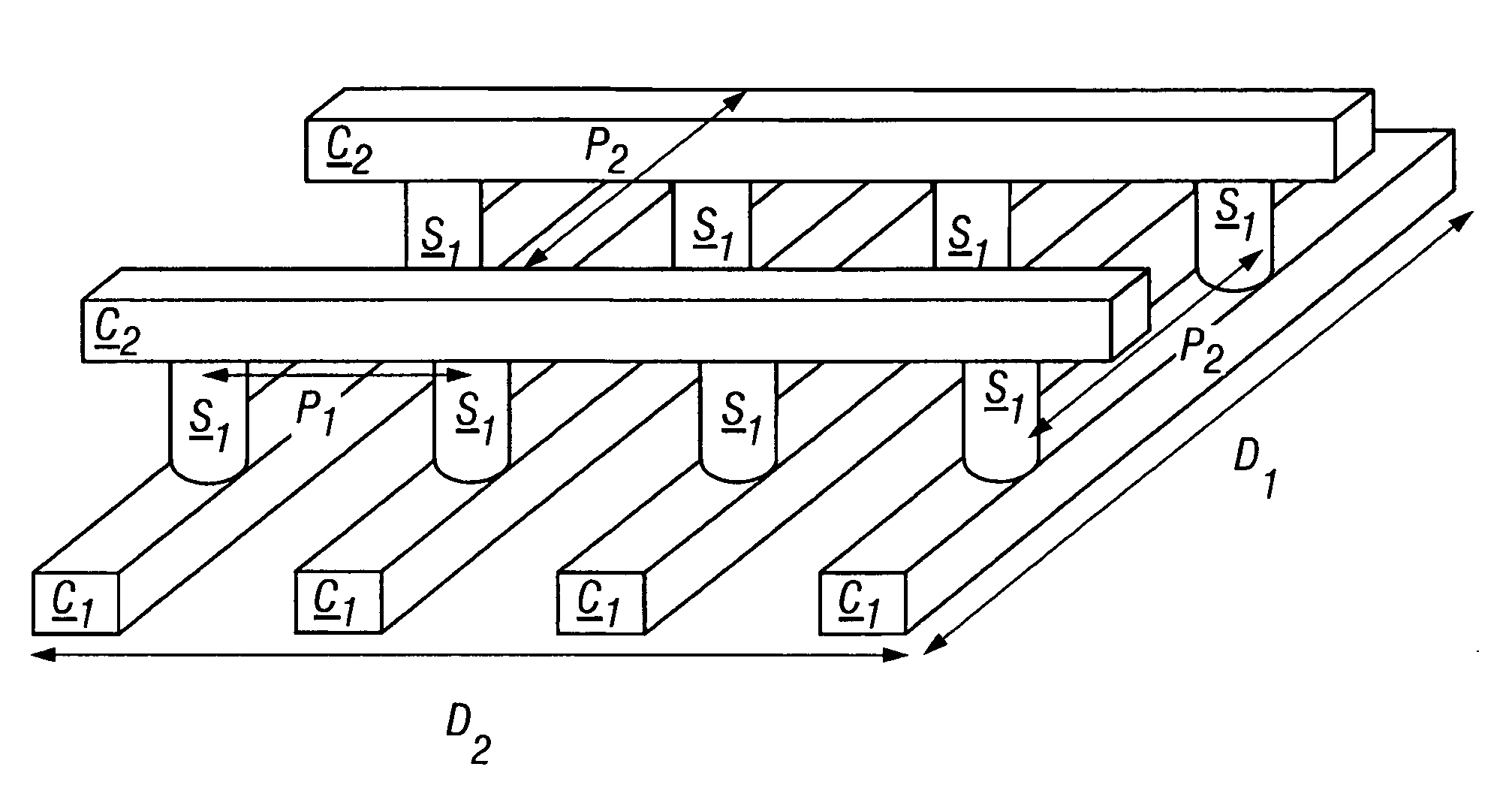
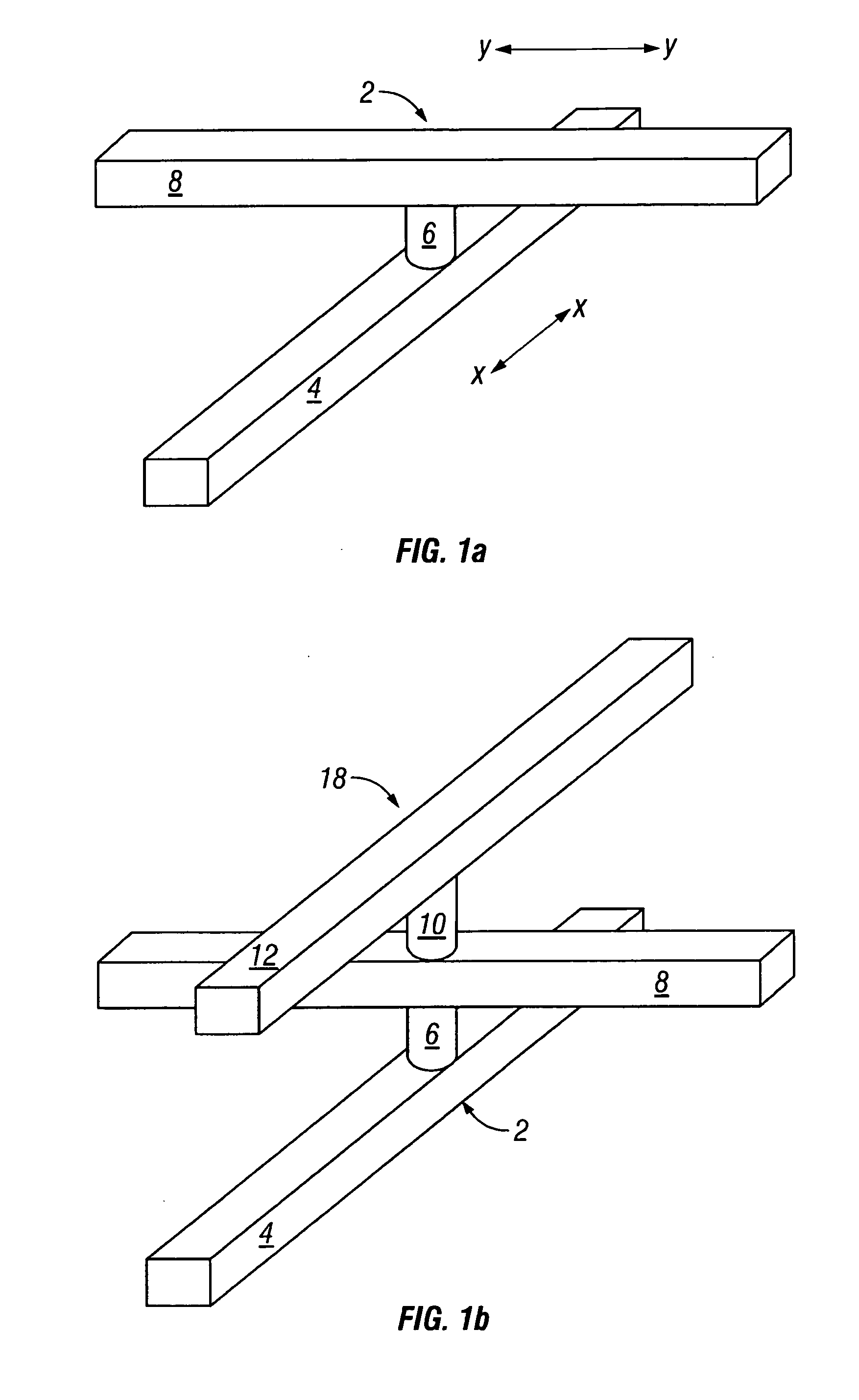
[0022] Johnson et al. and Knall et al. both disclose monolithic three dimensional memories which provide for high density memory arrays. The present invention provides for creation of a monolithic three dimensional memory with a structure similar to those disclosed in Johnson et al., but uses a different method of fabrication and different choice of materials, allowing for improved density, performance, and ease of manufacture.

[0023] The structure of a single memory cell 2 of the present invention is illustrated in FIG. 1a. At the bottom is conductor 4. Above conductor 4 is semiconductor element 6, and above that is conductor 8. In the present invention, semiconductor element 6 is substantially cylindrical, for reasons that will be described below. The memory cell of Johnson et al. has a similar structure, but its semiconductor element, called a pillar, is not substantially cylindrical. Turning to FIG. 1b, in both the memory of Johnson et al. and the present invention, another semi...


PUM


Abstract

An improved method for fabricating a three dimensional monolithic memory with increased density. The method includes forming conductors preferably comprising tungsten, then filling and planarizing; above the conductors forming semiconductor elements preferably comprising two diode portions and an antifuse, then filling and planarizing; and continuing to form conductors and semiconductor elements in multiple stories of memories. The arrangement of processing steps and the choice of materials decreases aspect ratio of each memory cell, improving the reliability of gap fill and preventing etch undercut.

Description

[0001] This application is a continuation of Herner et al., “An Improved Method for Making High-Density Nonvolatile Memory,” U.S. patent application Ser. No. 10 / 326,470, which is hereby fully incorporated into the instant patent application specification by reference. This application is related to the following applications, all continuations of Ser. No. 10 / 326,470, all filed on even date herewith and all assigned to the assignee of the present invention: Herner et al., “An Improved Method for Making High-Density Nonvolatile Memory,” (attorney docket number MA-086-a); Herner et al., “An Improved Method for Making High-Density Nonvolatile Memory,” (attorney docket number MA-086-b); Vyvoda et al., “Contacts for an Improved High-Density Nonvolatile Memory,” (attorney docket number MA-086-c); Herner et al., “An Improved Method for Making High-Density Nonvolatile Memory,” (attorney docket number MA-086-d); Herner et al., “An Improved Method for Making High-Density Nonvolatile Memory,” (...

Claims


Application Information

Patent Timeline
IPC IPC(8): G11CG11C5/02H01L21/00H01L21/331H01L21/82H01L21/8238H01L23/48H01L27/102H01L27/148H01L29/94H01L31/0392H01L31/119
CPCH01L27/1021H01L21/02518H01L2924/0002H01L2924/00H01L27/148G11C5/02H01L21/8238H01L23/48H01L29/94
Inventor HERNER, S. BRADMAHAJANI, MAITREYEE
Owner SANDISK TECH LLC
Why Eureka
Try Eureka