Electrical terminal

Inactive Publication Date: 2005-06-16
HON HAI PRECISION IND CO LTD
10 Cites 7 Cited by

AI-Extracted Technical Summary

Problems solved by technology

However, in application, the gold fingers of the electronic card tend to be stained by dielectric material.
Certainly, this will adv...

Benefits of technology

[0006] Accordingly, an object of the present invention is to provide an improved terminal having a contacting...

Abstract

An electrical terminal (1) is received in an insulating housing (21) of an electrical connector (2). The electrical terminal (1) includes a contacting portion (2), a soldering portion (13), a retaining portion (12) retained in the insulating housing (21) and a coupling portion (14) connecting with the contacting portion (11) and the soldering portion (13). The contacting portion (11) defines a contacting point (110) adjacent to a tip end thereof. The contacting point (110) includes an upper section (111) and a lower section (112) wider than the upper section (111). As a result, the contacting point (110) is in a form of blade.

Application Domain

Technology Topic

Image

  • Electrical terminal
  • Electrical terminal
  • Electrical terminal

Examples

  • Experimental program(1)

Example

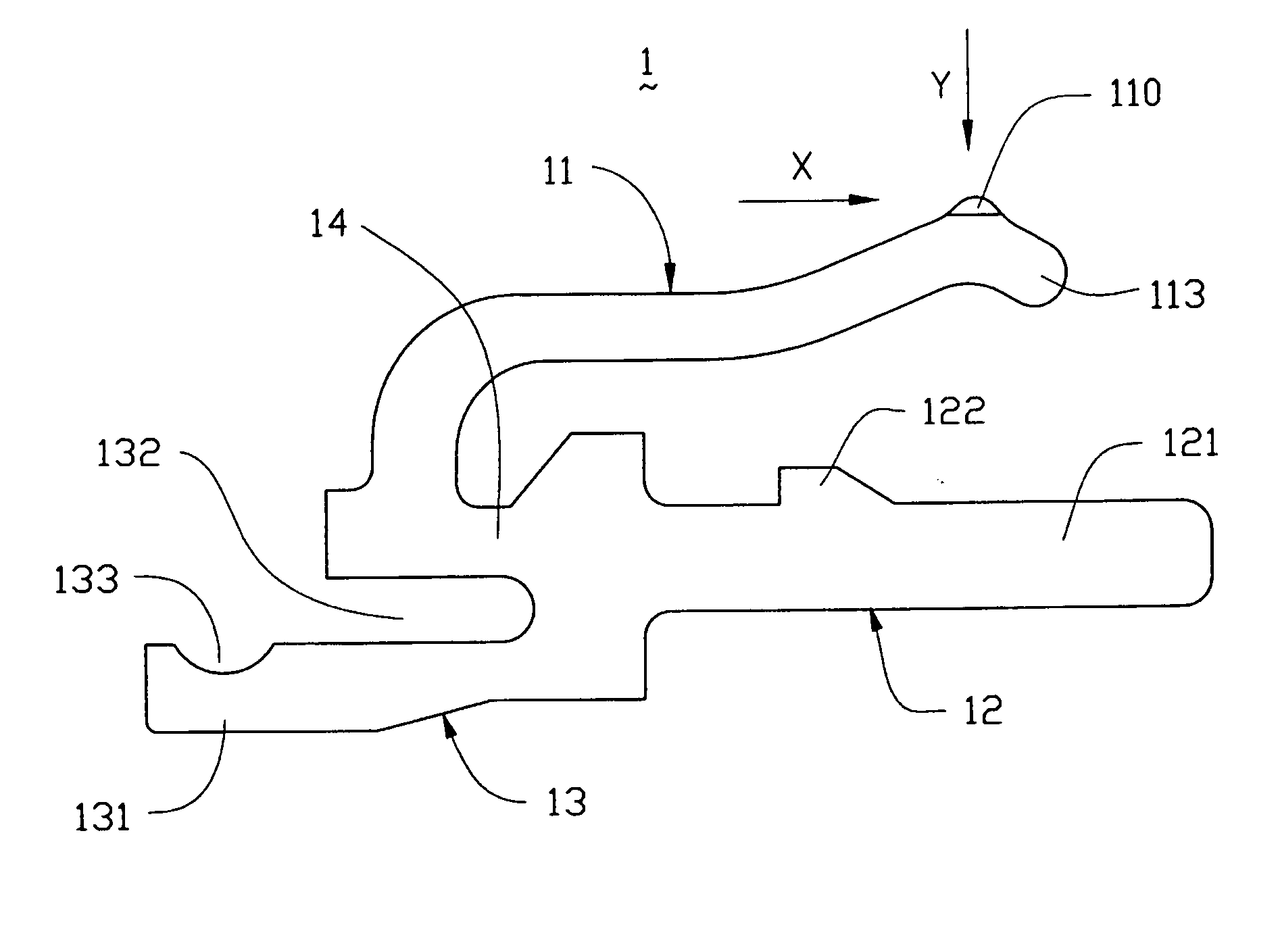
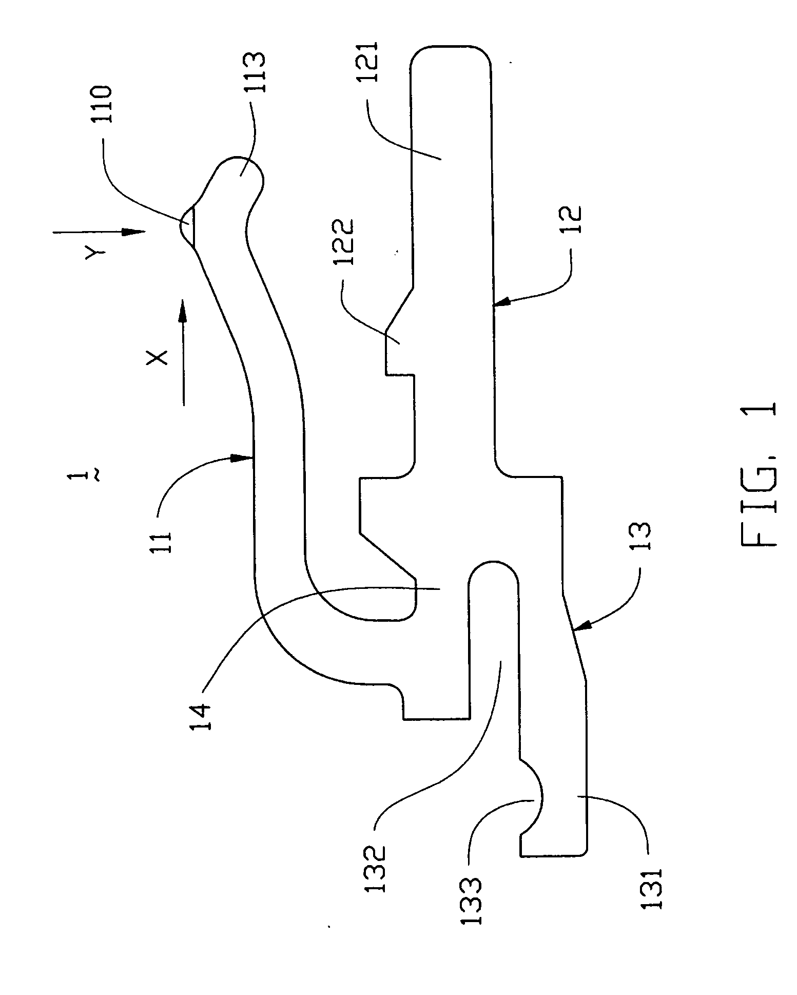
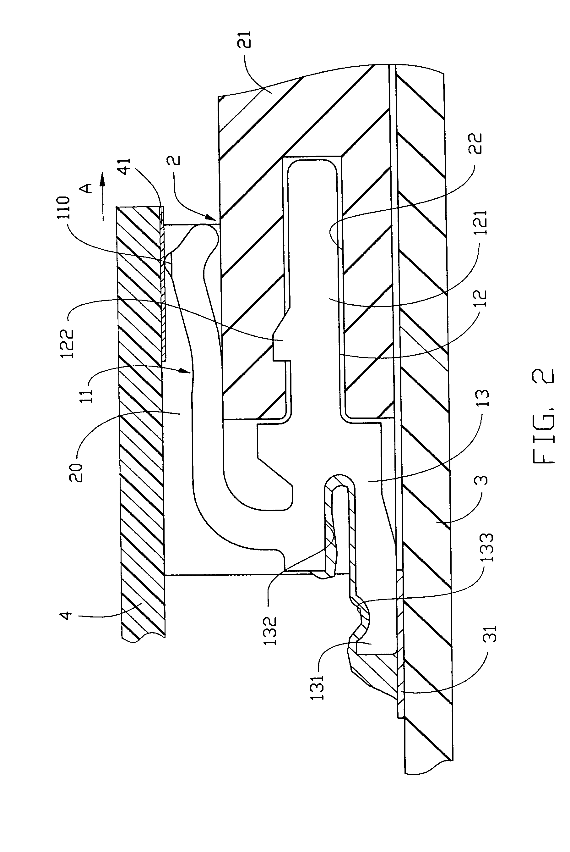
[0013] Referring to FIGS. 1 and 2, in this embodiment, an electrical terminal 1 in accordance with the present invention comprises a contacting portion 11, a soldering portion 13, a coupling portion 14 connecting the contacting portion 11 and the soldering portion 13, and a retaining portion 12 protruding from the coupling portion 14 and extending between the contacting portion 11 and the soldering portion 13. The contacting portion 11 defines a contacting point 110 adjacent to a tip end 113 thereof. The soldering portion 13 defines a soldering tail 131 extending in a direction opposite to an extending direction of the contacting portion 11. The tail 131 is surface mounted to a contact pad 31 formed on a printed circuit board (PCB). The retaining portion 12 is opposed to and parallel to the soldering portion 13. The retaining portion 12 similarly parallels the contacting portion 11 and has a protrusion beam 121 engaging with an insulating housing 21 of an electrical connector 2. The protrusion beam 121 forms a barb 122 on a top edge thereof for engaging with the housing 21 interferentially. A guiding slot 132 is defined between the soldering tail 131 and the contacting portion 11 opposite to the retaining portion 12. Furthermore, a cutout 133 is defined on an edge of the soldering tail 131 adjacent to the guiding slot 132.
[0014] Turning to FIG. 2, the contacting portion 11 of the terminal 1 is received in a passageway 20 defined in the housing 21 of the electrical connector 2. The protrusion beam 121 of the retaining portion 12 enters an engaging hole 22 defined in the housing 21. The barb 122 of the retaining portion 12 hooks the inner face of the engaging hole 22 so that the electrical terminal 1 is retained in the housing 21 firmly. After the connector 2 is mounted on a proper position on the PCB 3, the solder tail 131 is soldered to the contact pad 31 formed on the PCB 3. Then an electronic component 4 is inserted into the housing along a direction A. The mating portion 41 of the electronic component 4 can slip on the contacting point 110 of the electrical terminal 1 along the direction A.
[0015] Together referring to FIGS. 3 and 4, the contacting point 110 includes an upper section 111 and a lower section 112. The width d of the upper section 111 is smaller than the width D of the lower section 112, which results in that the contacting point 110 is in a form of blade. When the mating portion 41 of the electronic component 4 slipping on the contacting point 110 along the direction A, the contacting point 110 can scraped the mating portion 41. If dielectric materials stain the mating portion 41, the contacting point 110 in the form of blade can scrap the dielectric material off the mating portion 41. In this condition, the electrical terminal 1 electrically connected with the corresponding electronic component 4 reliably.
[0016] It is to be understood, however, that even though numerous characteristics and advantages of the present invention have been set forth in the foregoing description, together with details of the structure and function of the invention, the disclosure is illustrative only, and changes may be made in detail, especially in matters of shape, size, and arrangement of parts within the principles of the invention to the full extent indicated by the broad general meaning of the terms in which the appended claims are expressed.

PUM

no PUM

Description & Claims & Application Information

We can also present the details of the Description, Claims and Application information to help users get a comprehensive understanding of the technical details of the patent, such as background art, summary of invention, brief description of drawings, description of embodiments, and other original content. On the other hand, users can also determine the specific scope of protection of the technology through the list of claims; as well as understand the changes in the life cycle of the technology with the presentation of the patent timeline. Login to view more.

Similar technology patents

Test element analysis system

Owner:ROCHE DIAGNOSTICS OPERATIONS

Wire with terminal and manufacturing method therefor

ActiveUS20170331243A1Electrical connection be ensureElectrical resistance decreaseSoldered/welded connectionsConnections effected by permanent deformationEngineeringElectrical and Electronics engineering
Owner:AUTONETWORKS TECH LTD +3

Magnetic head device and method for making the same

InactiveUS20050030667A1Good electrical connectionElectrical connection be ensureHeads using thin filmsRecord information storageJoint surfaceEngineering
Owner:TDK CORPARATION

Classification and recommendation of technical efficacy words

  • Electrical connection be ensure

End-loaded battery carriage

Owner:MICROSOFT TECH LICENSING LLC

Wire with terminal and manufacturing method therefor

ActiveUS20170331243A1Electrical connection be ensureElectrical resistance decreaseSoldered/welded connectionsConnections effected by permanent deformationEngineeringElectrical and Electronics engineering
Owner:AUTONETWORKS TECH LTD +3

Magnetic head device and method for making the same

InactiveUS20050030667A1Good electrical connectionElectrical connection be ensureHeads using thin filmsRecord information storageJoint surfaceEngineering
Owner:TDK CORPARATION
Why Eureka
Try Eureka