

Method of forming a projection electrode
- Summary
- Abstract
- Description
- Claims
- Application Information
AI Technical Summary
Benefits of technology
Problems solved by technology
Method used
Image

Examples
second embodiment
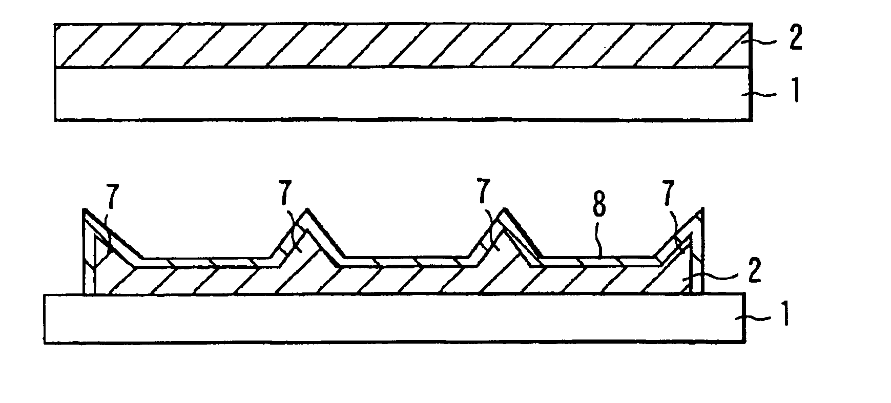
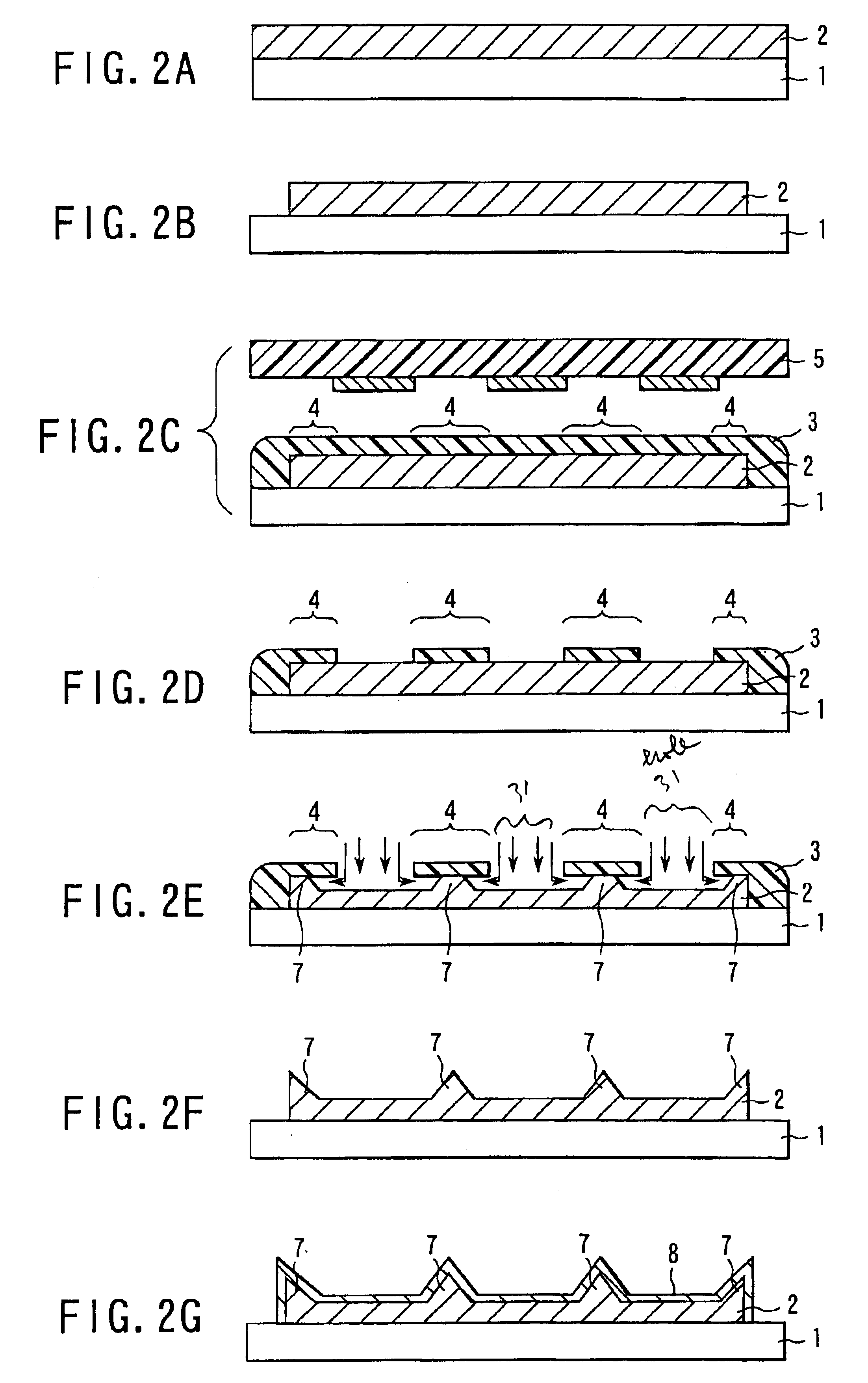
[0038]FIG. 5 is a perspective view showing a wiring board 1 equipped with projection electrodes 7 having bump configurations, the projection electrode corresponding to the present invention. The projection electrodes 11 formed on the wiring board 1 with the same process as set out above, are formed in a manner to be connected to a circuit pattern 10 and equipped with ridge bumps 7b having a pointed tapering end in vertical cross-section. In this embodiment, the pointed tapering end is adapted to be linearly connected to an associated electrode and ensures a positive electrical connection to the associated electrode with less connection resistance at the time of connection. It is, therefore, possible to reduce the pressing force of a semiconductor chip with which the chip is mounted. The shape of the projection electrode 11 can be freely determined by changing the process conditions of the thickness and material of the DF 3, composition components of an etching solution or temperatur...
third embodiment
[0040]the present invention will be described, with reference to FIGS. 7 to 14.
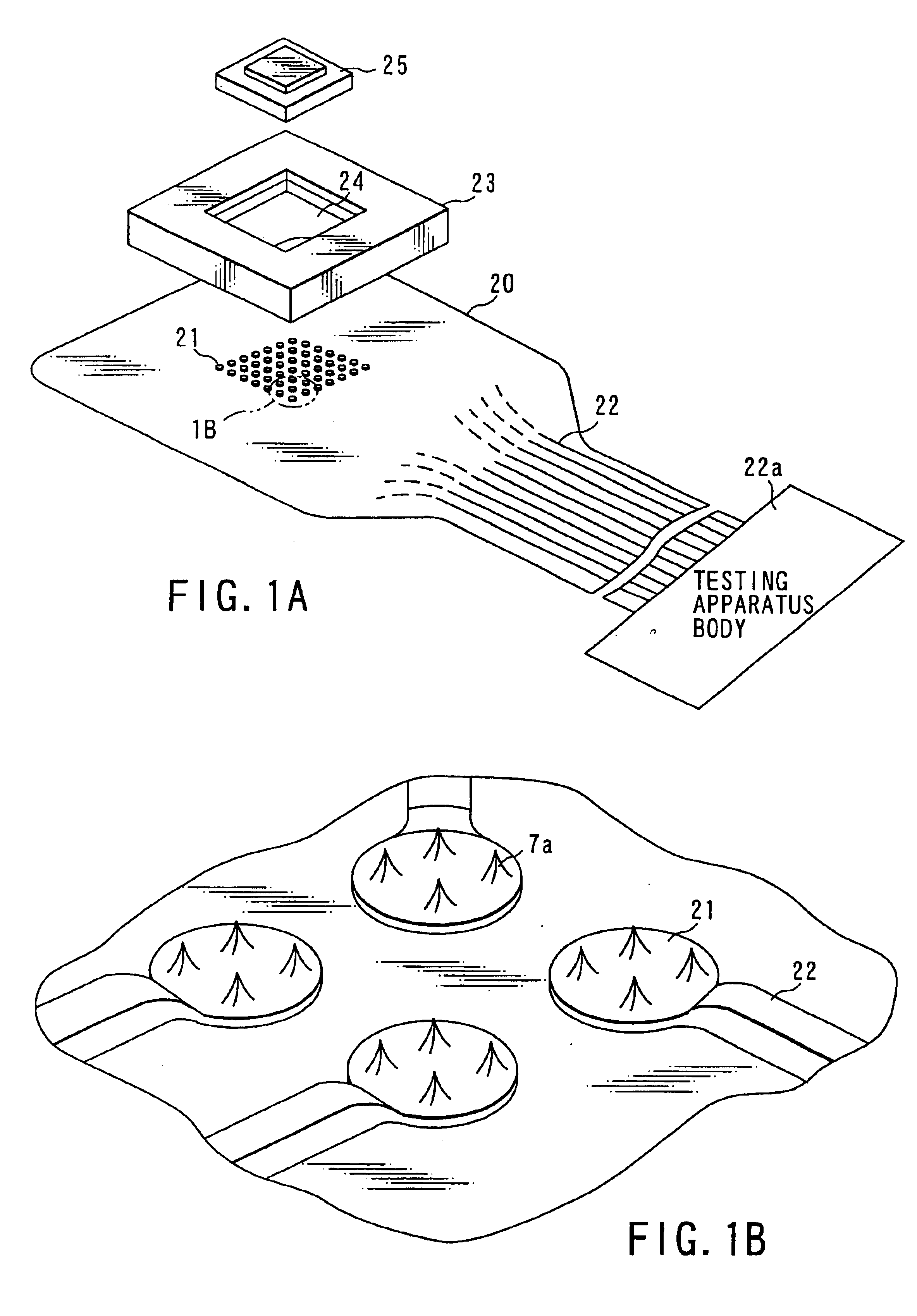
[0041]FIG. 7 shows a part of a testing apparatus for testing electronic components. FIG. 8A is a magnified perspective view of a part of the testing apparatus, on which one projection electrode 51 according to the that the projecting electrodes 51 protrude upwards in the square opening. The square opening defines a chip-holding recess 54. In the recess 54, a chip-sized package (CSP) 55, for example, is placed with its electrodes extending downwards. Thus, the electrodes of the CSP 55 are directly connected to the bumps 67 of the projection electrodes 51.
[0042]As shown in FIG. 8B, the bumps 67 of each projection electrode 51 comprise projections 41 and a metal layer 42. The projections 41 are formed integral with the insulating layer 40 of the wiring board 50. The metal layer 42 covers the projections 41. The metal layer 42 is composed of two metal layers 61 and 62. The first metal layer 61 covers the insu...
PUM
| Property | Measurement | Unit |
|---|---|---|
| Corrosion properties | aaaaa | aaaaa |
| Electrical conductor | aaaaa | aaaaa |
| Area | aaaaa | aaaaa |
Abstract
Description
Claims
Application Information