Field emission device, display adopting the same and method of manufacturing the same

a field emission device and display technology, applied in the field of field emission devices, can solve the problems of deteriorating color purity, difficult application of disclosed feed to a large-screen display field, and inability to precisely display the desired color at a given pixel, etc., to achieve the effect of improving the focusing of electron beams

Inactive Publication Date: 2005-06-23
SAMSUNG SDI CO LTD
View PDF38 Cites 37 Cited by
  • Summary
  • Abstract
  • Description
  • Claims
  • Application Information

AI Technical Summary

Benefits of technology

[0012] The present invention provides a field emission device which has improved focusing of electron beams, a display adopting the same, and a method of manufacturing the same. In an aspect of the present invention, there is provided a field emission device having a glass substrate, an emitter electrode formed on the glass substrate, a carbon nanotube (CNT) emitter formed on the emitter electrode, and a gate stack formed around the CNT emitter for extracting electron beams from the CNT emitter and focus...

Problems solved by technology

In the field emission display having the above-described structure, however, if the trajectories of electron beams are not controlled, a desired color cannot be exactly displayed at a given pixel.
Overfocused electrons deviate from a target phosphor layer region and excite a phosphor layer in another region, which results in deterioration of color...

Method used


Image

  • Field emission device, display adopting the same and method of manufacturing the same
  • Field emission device, display adopting the same and method of manufacturing the same
  • Field emission device, display adopting the same and method of manufacturing the same

Examples


Embodiment Construction

[0030] A field emission display device according to the present invention, a display device adopting the same, and a method of manufacturing the same will now be described more fully hereinafter with reference to the accompanying drawings, in which preferred embodiments of the invention are shown. In the drawings, the thickness of layers, regions, etc. are exaggerated for clarity.

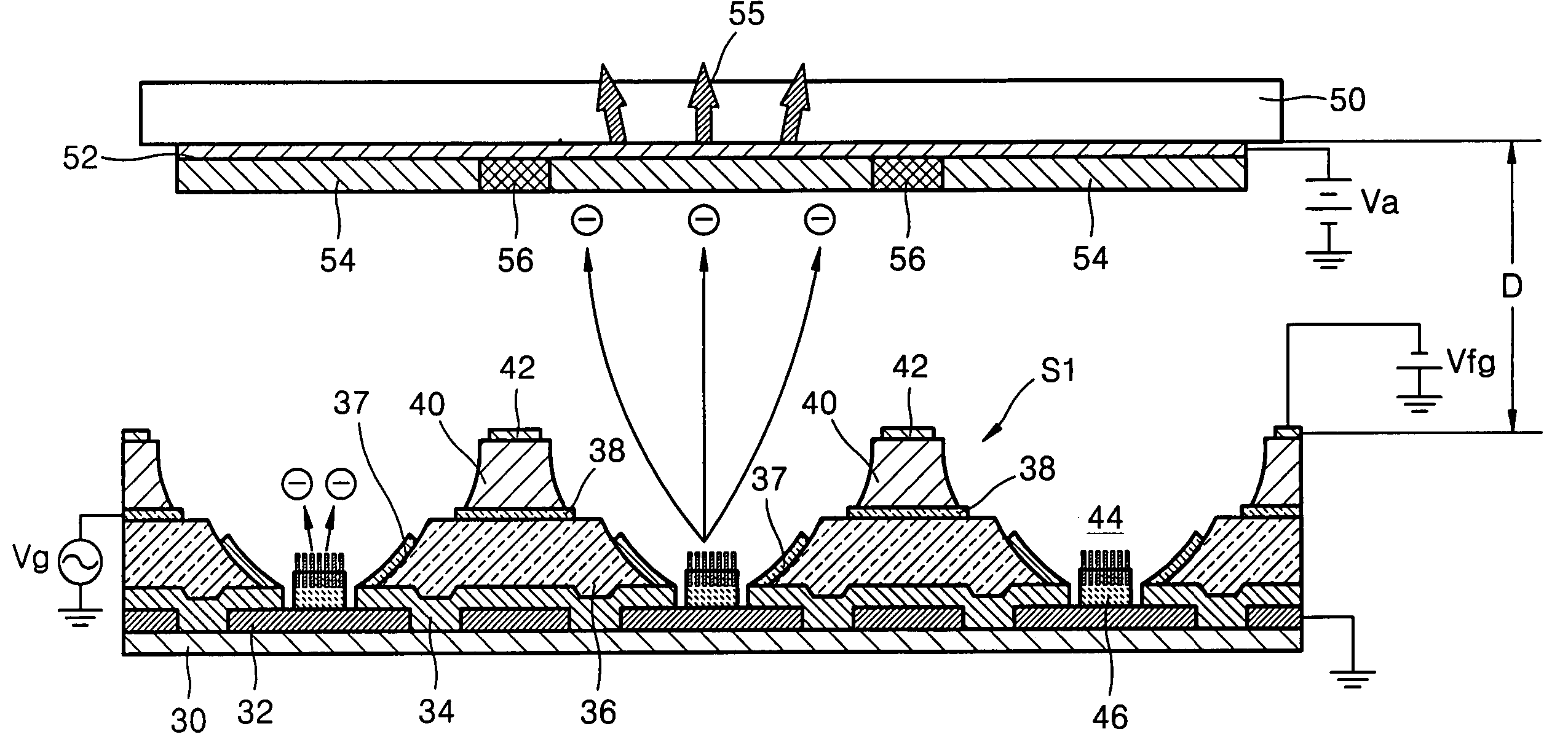
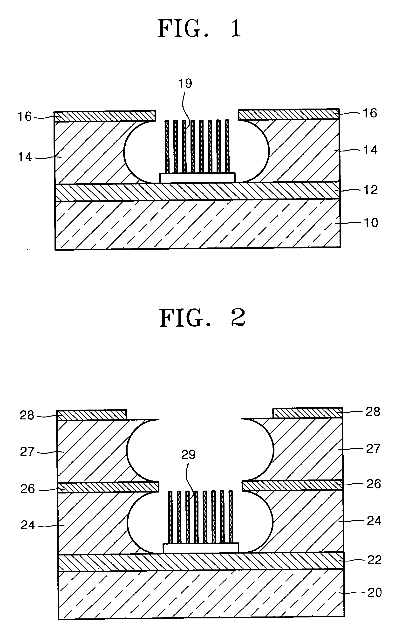
[0031]FIG. 1 is a schematic diagram of a field emission display device. Referring to FIG. 1, the field emission display device includes a cathode 12 formed on a substrate 10. Also, a gate electrode 16 is formed as an electron extracting electrode on an insulating layer 14. A field emitter 19 is provided within a hole through which part of the cathode 12 is exposed.

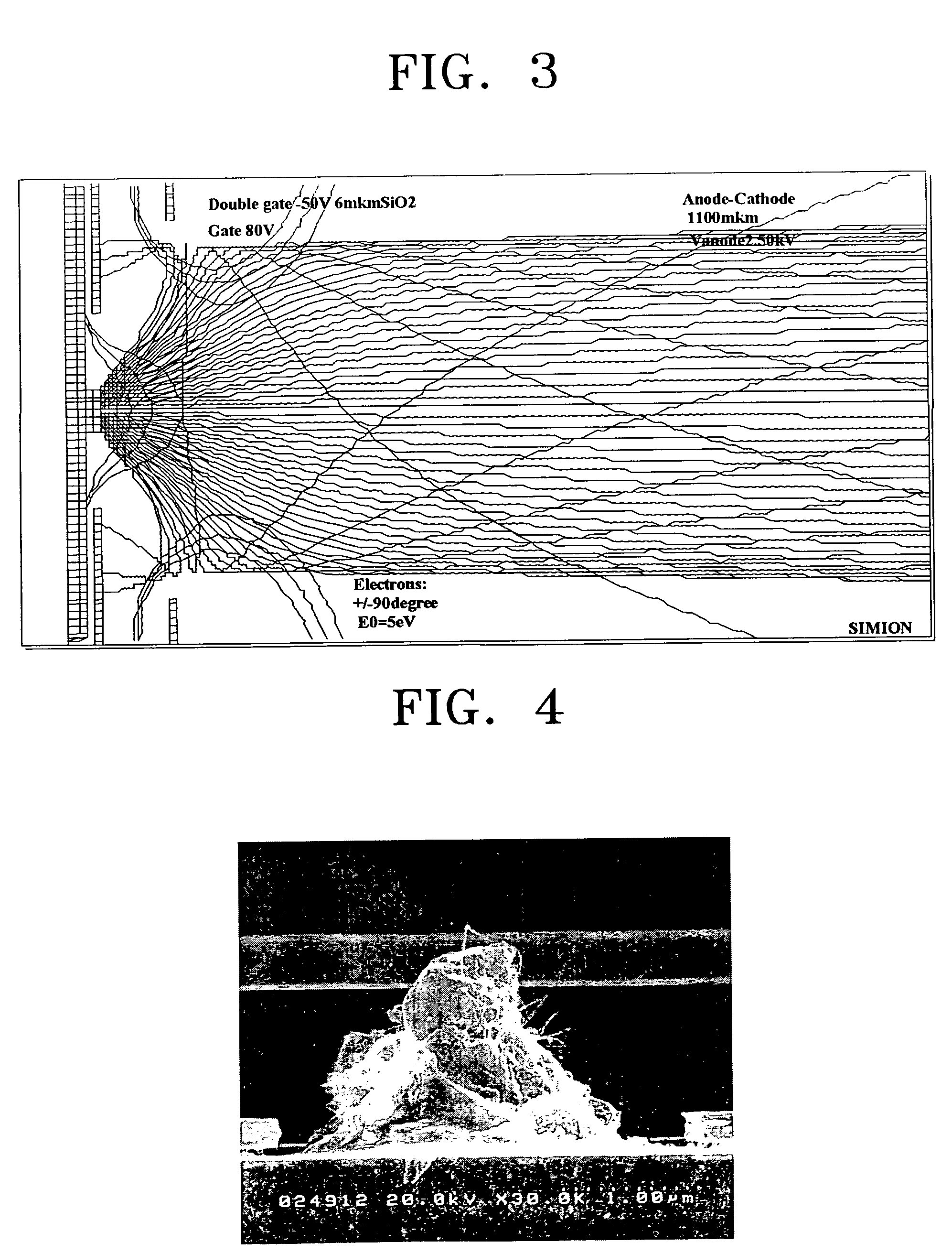
[0032] In the field emission display device having the above-described structure, however, if trajectories of electron beams are not controlled, a desired color cannot be exactly displayed at a given pixel. Therefore, there is a demand for an el...


PUM


Abstract

A field emission device comprises a glass substrate, an emitter electrode formed on the glass substrate, a carbon nanotube (CNT) emitter formed on the emitter electrode, and a gate stack formed around the CNT emitter for extracting electron beams from the CNT emitter and focusing the extracted electron beams onto a given position. The gate stack includes a mask layer covering the emitter electrode and provided around the CNT emitter, a gate insulating layer formed on the mask layer to a predetermined height, a mirror electrode formed on an inclined plane of the gate insulating layer, a gate electrode formed on the gate insulating layer and spaced apart from the mirror electrode, and a focus gate insulating layer and a focus gate electrode sequentially formed on the gate electrode. The field emission device is manufactured and employed in a display device in accordance with the present invention.

Description

CLAIM OF PRIORITY [0001] This application makes reference to, incorporates the same herein, and claims all benefits accruing under 35 U.S.C. § 119 from an application for FIELD EMISSION DEVICE, DISPLAY ADOPTING THE SAME AND METHOD OF MANUFACTURING THE SAME earlier filed in the Korean Intellectual Property Office on 22 Dec. 2003 and there duly assigned Serial No. 2003-94415. BACKGROUND OF THE INVENTION [0002] 1. Technical Field [0003] The present invention relates to a field emission device, a display adopting the same, and a method of manufacturing the same and, more particularly, to a field emission device which has improved focusing effect of electron beams, a display adopting the same, and a method of manufacturing the same. [0004] 2. Related Art [0005] Display devices, which are the principal conventional information transmission media, have been typically used as monitors of PCs and TV receivers. Such display devices are largely classified into cathode ray tubes (CRTs) which us...

Claims


Application Information

Patent Timeline
IPC IPC(8): H01J29/04H01J1/30H01J1/304H01J3/02H01J9/02H01J29/46H01J29/48H01J31/12H01L21/00H01L29/06
CPCB82Y10/00H01J3/022H01J9/025Y10S977/939H01J2201/30469H01J2329/00H01J29/481H01J1/30
Inventor CHOI, JUN-HEEZOULKARNEEV, ANDREI
Owner SAMSUNG SDI CO LTD
Why Eureka
Try Eureka