Field emission display (FED) and method of manufacture thereof

a field emission display and field emission technology, applied in the manufacture of electric discharge tubes/lamps, discharge tubes with screens, discharge tubes luminescnet screens, etc., can solve the problems of increasing the production cost of feds, and preventing the reduction of current density, so as to improve electron beam focusing

Inactive Publication Date: 2005-12-01
SAMSUNG SDI CO LTD
View PDF3 Cites 22 Cited by
  • Summary
  • Abstract
  • Description
  • Claims
  • Application Information

AI Technical Summary

Benefits of technology

[0019] The present invention provides a Field Emission Display (FED) having an electron emitting structure which improves electron beam focusing and prevents a decrease in current density, and a method of manufacture thereof.

Problems solved by technology

Thus, the manufacturing process is complicated and expensive equipment has to be used, thereby increasing the production costs of the FED.
Accordingly, an FED having the metal tip emitter cannot be used for large screens.
However, the FED having the triode structure as described above has low color purity during driving and has difficulty in obtaining a clear image.
These problems occur because most electrons are emitted from an edge portion of the emitter and an electron beam proceeding toward the fluorescent layer diverges due to the voltage (a positive voltage of several volts through tens of volts) supplied to the gate electrode, thereby allowing a phosphor of adjacent other pixel as well as a phosphor of the intended pixel to emit light.
However, it is difficult to form a number of emitters in a pixel of a predetermined size and the entire area of the emitters for allowing a phosphor of the concerned pixel to emit light decreases.
Also, the effect of focusing the electron beam is not sufficient.
However, these FEDs have complicated structures.
Also, since the above structures have been mainly applied to a FED having a metal tip emitter formed on the cathode, when the structures are applied to a FED having flat shape emitter, a satisfactory effect has not yet been obtained.
Thus, the structure is very complicated so that manufacturing is difficult and the structure is also spatially limited.
Accordingly, there is a limitation in maximizing the number and the area of the emitter with respect to one pixel, thereby shortening the lifetime.

Method used


Image

  • Field emission display (FED) and method of manufacture thereof
  • Field emission display (FED) and method of manufacture thereof
  • Field emission display (FED) and method of manufacture thereof

Examples


Embodiment Construction

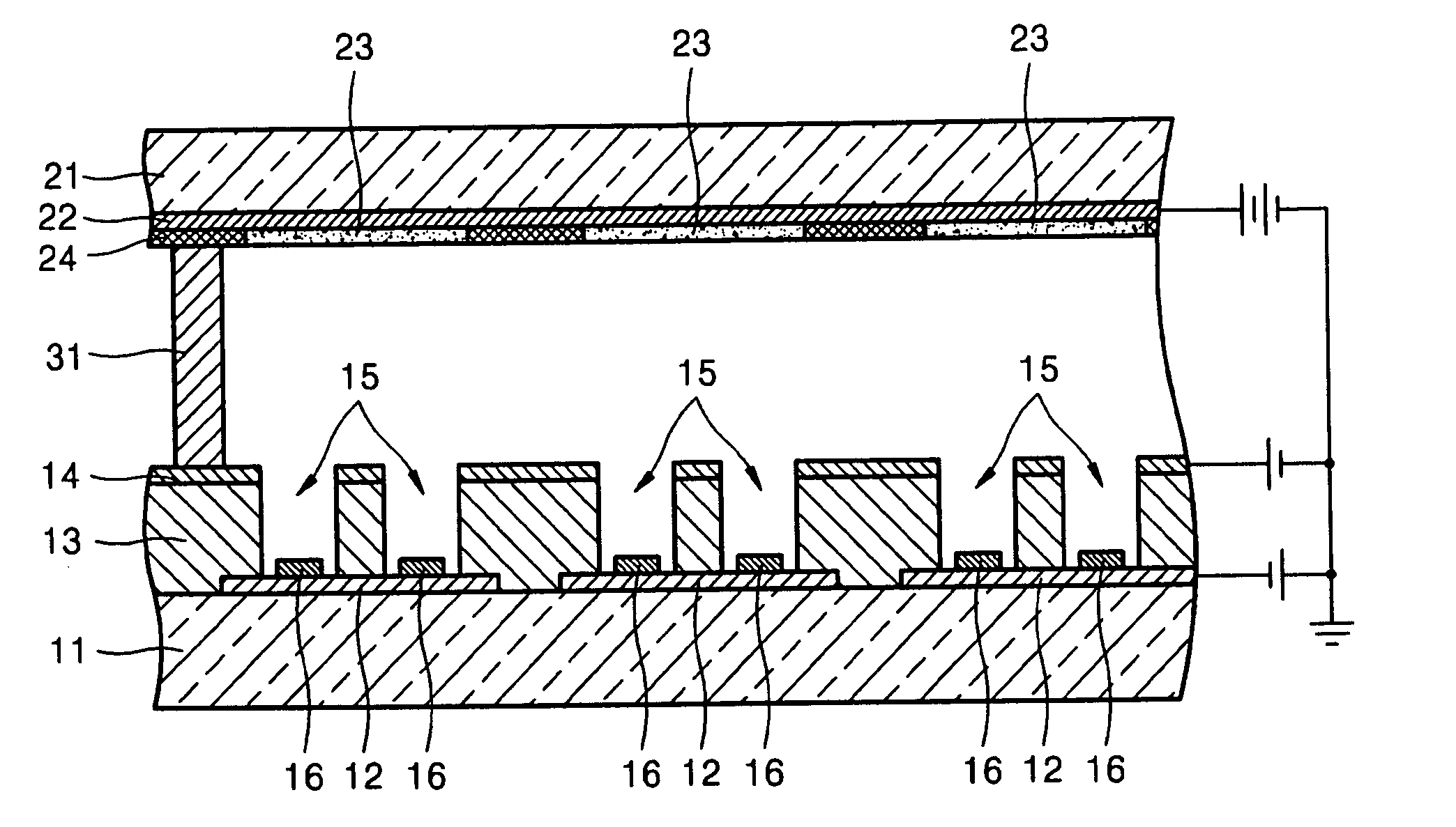
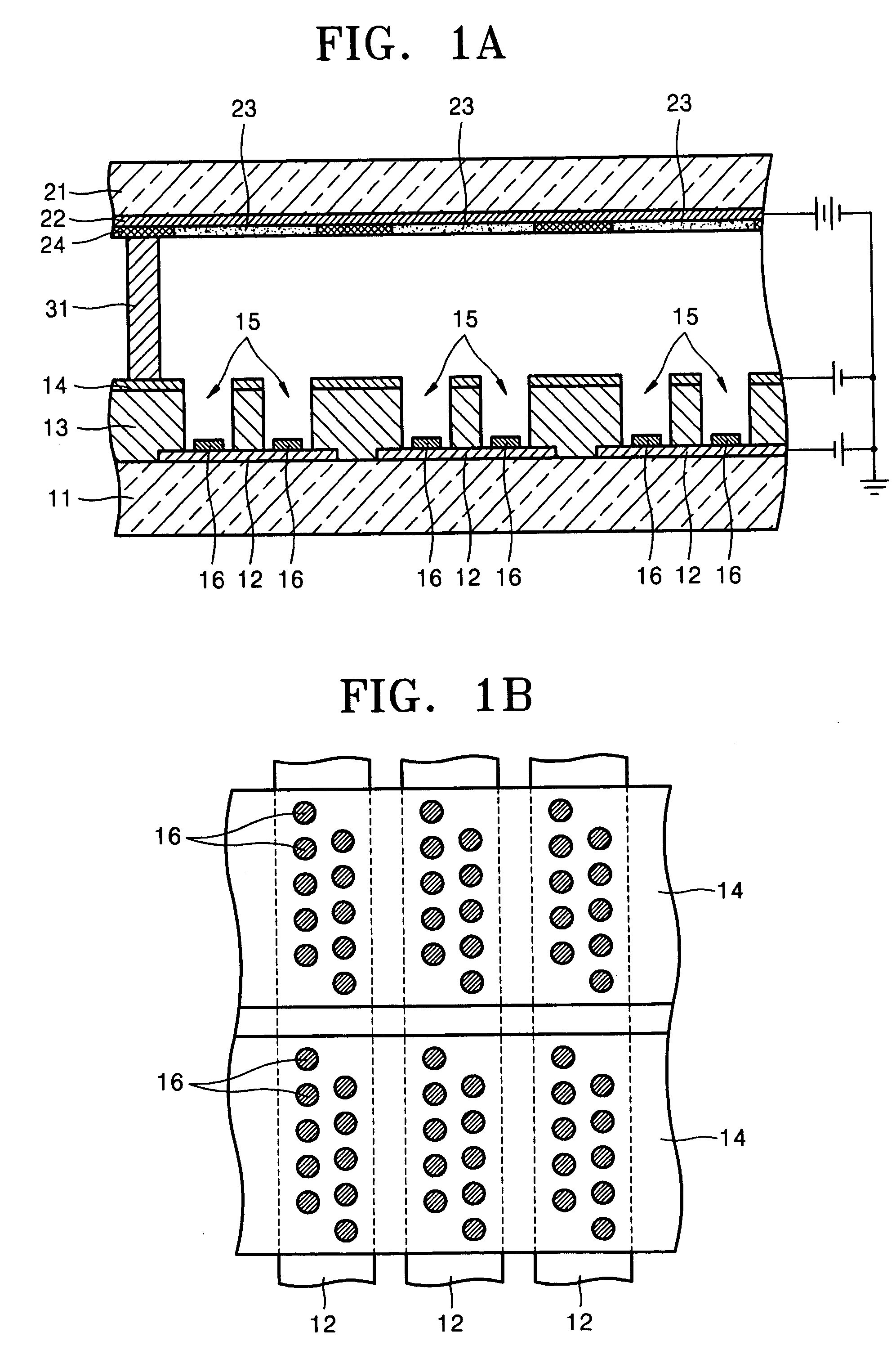
[0078]FIGS. 1A and 1B are views of an FED, FIG. 1A is a partial cross-sectional view of the FED and FIG. 1B is a partial plan view of the FED.

[0079] Referring to FIGS. 1A and 1B, the FED has a triode structure including a cathode 12, an anode 22, and a gate electrode 14. The cathode 12 and the gate electrode 14 are formed on a rear substrate 11 and the anode 22 is formed on a lower surface of a front substrate 21. Fluorescent layers 23, composed of R, G, and B phosphors, and a black matrix 24 for improving contrast are formed on the lower surface of the anode 22. The rear substrate 11 and the front substrate 21 are spaced from each other by a spacer 31 arranged therebetween. In such an FED, the cathode 12 is first formed on the rear substrate 11, an insulating layer 13 and the gate electrode 14 which have fine openings 15 are stacked thereon, and then emitters 16 are arranged on the cathode 12 located in the openings 15.

[0080] However, the FED having the triode structure as descri...


PUM


Abstract

A Field Emission Display (FED) includes: a first substrate; a first insulating layer arranged on the first substrate; a cathode arranged on the first substrate to cover the first insulating layer, the cathode having a first concave opening arranged between portions thereof covering the first insulating layer: a second insulating layer arranged on the first substrate and the cathode, the second insulating layer having a second opening connected to the first opening to expose a portion of the cathode; a gate electrode arranged on the second insulating layer, the gate electrode having a third opening connected to the second opening; a plurality of emitters arranged on the cathode in the first opening and along both edges of the first opening and spaced apart from each other; and a second substrate facing the first substrate and spaced apart therefrom and having an anode and a fluorescent layer arranged on a surface thereof.

Description

CROSS-REFERENCE TO RELATED APPLICATIONS [0001] Furthermore, the present application is related to a co-pending U.S. applications, Ser. No. (to be determined), entitled FIELD EMISSION DISPLAY AND METHOD OF MANUFACTURING THE SAME, based upon Korean Patent Application Serial No. 10-2004-0036672 filed in the Korean Intellectual Property Office on May 22, 2004, and filed in the U.S. Patent & Trademark Office concurrently with the present application.CLAIM OF PRIORITY [0002] This application makes reference to, incorporates the same herein, and claims all benefits accruing under 35 U.S.C. § 119 from an application for FIELD EMISSION DISPLAY AND METHOD OF MANUFACTURING THE SAME earlier filed in the Korean Intellectual Property Office on May 29, 2004 and there duly assigned Serial No. 10-2004-0038720. BACKGROUND OF THE INVENTION [0003] 1. Field of the Invention [0004] The present invention relates to a Field Emission Display (FED) having an electron emitting structure which improves electro...

Claims


Application Information

Patent Timeline
Patent Type & Authority Applications(United States)
IPC IPC(8): H01J29/04H01J1/30H01J1/304H01J9/02H01J29/48H01J29/50H01J31/12
CPCH01J31/127H01J29/481
Inventor OH, TAE-SIK
Owner SAMSUNG SDI CO LTD
Why Eureka
Try Eureka