Flat panel display and method of manufacturing the same

Inactive Publication Date: 2005-06-23
SAMSUNG SDI CO LTD
View PDF2 Cites 13 Cited by
  • Summary
  • Abstract
  • Description
  • Claims
  • Application Information

AI Technical Summary

Benefits of technology

[0009] The present invention is directed to a flat panel display with strengthened adhesion of the anode to the second substrate. This strengthened adhesio

Problems solved by technology

Instead, the metallic material is intermittently broken, making it difficult to form a uniform metallic film.
Accordingly, the adhesion of the anode to the second substrate is significantly weakened, and a stable anode is difficult to form.
As a result, the anode is likely to be damaged at the

Method used


Image

  • Flat panel display and method of manufacturing the same
  • Flat panel display and method of manufacturing the same
  • Flat panel display and method of manufacturing the same

Examples


Embodiment Construction

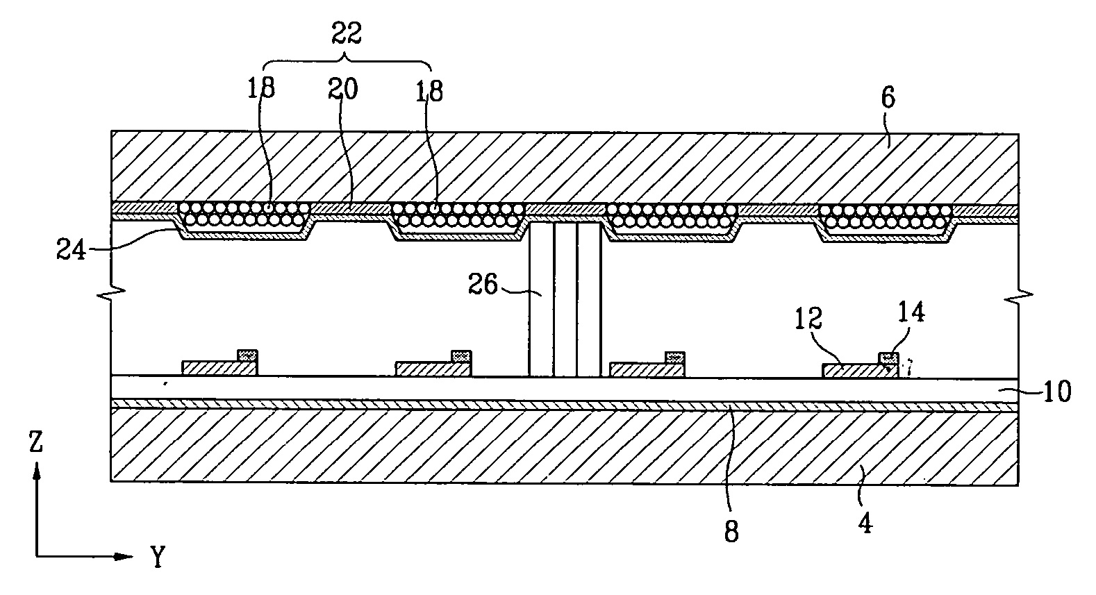
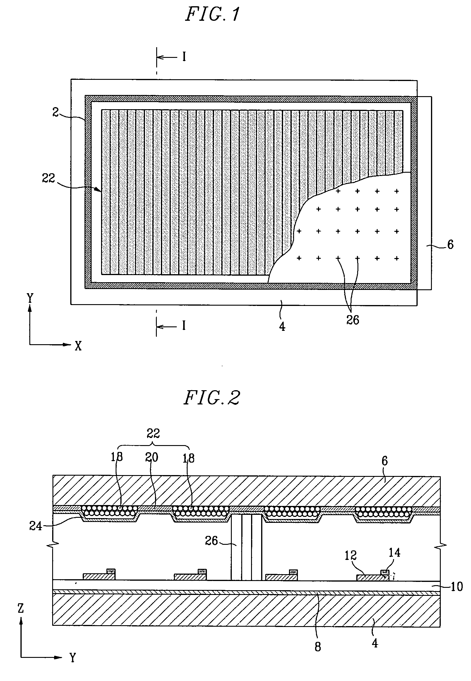
[0032]FIGS. 1 and 2 illustrate a flat panel display using FEA type electron emission sources. As shown, the flat panel display comprises a first substrate 4 and a second substrate 5 sealed together by a frit seal 2 to form a vacuum vessel. An electron emission unit is formed on the first substrate 4. The electron emission unit emits electrons which form visible rays at the second substrate 6, which then display the desired images.

[0033] Specifically, as shown in FIG. 2, gate electrodes 8 are formed on the first substrate 4 in a striped pattern, each gate electrode 8 proceeding in the Y direction. An insulating layer 10 is formed on the surface of the first substrate 4 covering the gate electrodes 8. Cathodes 12 are formed over the insulating layer 10 in a striped pattern, each cathode 12 proceeding in the X direction, perpendicular to the direction of the gate electrodes 8.

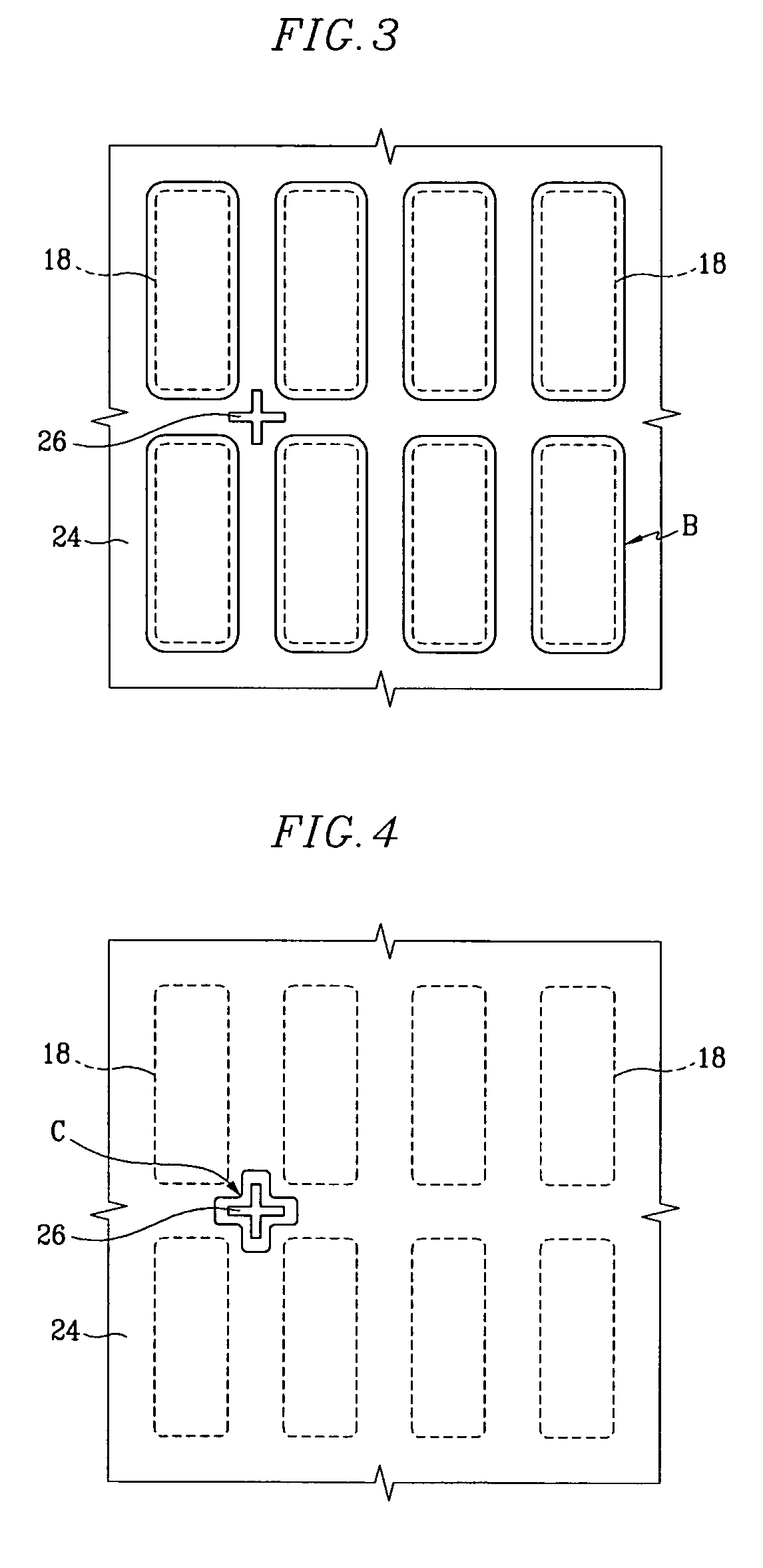
[0034] The regions where the gate electrodes 8 cross the cathodes 12 are defined as pixel regions. Electron e...


PUM


Abstract

A flat panel display with improved adhesion of the anode to the second substrate is disclosed. The adhesion of the anode to the second substrate is reinforced to prevent damage to the anode at the spacer formation area and to stably adhere the phosphor layer to the anode. The flat panel display comprises first and second substrates each facing each other and separated from each other by a distance. An electron emission unit is formed on the first substrate. A plurality of phosphor layers are formed on the second substrate. An anode is formed on the second substrate covering the phosphor layers and the non-light emitting regions between the phosphor layers. In the non-light emitting regions, the anode is placed on the second substrate without leaving a gap between the anode and the second substrate.

Description

CROSS-REFERENCE TO RELATED APPLICATION [0001] This application claims priority of Korean Patent Application number 10-2003-0085474, filed Nov. 28, 2003, the entire disclosure of which is incorporated herein by reference. FIELD OF THE INVENTION [0002] The present invention is directed to a flat panel display, and more particularly to a flat panel display exhibiting strengthened adhesion of the anode to the substrate having phosphor layers. BACKGROUND OF THE INVENTION [0003] Generally, a flat panel display includes a vacuum vessel having first and second substrates, each facing the other and separated from each other by a distance. Spacers are formed between the first and second substrates. In a flat panel display, electrons are emitted from electron emission sources located on the first substrate. These emitted electrons then collide with phosphor layers located on the second substrate. These collisions emit light and thereby display the desired images. [0004] The electron emission s...

Claims


Application Information

Patent Timeline
IPC IPC(8): H01J9/22H01J1/30H01J1/62H01J9/02H01J29/02H01J29/08H01J29/28H01J29/32H01J29/86H01J29/87H01J31/12H01J31/15H01J63/04
CPCH01J29/085H01J2329/863H01J31/127H01J29/864H01J1/30
Inventor HWANG, SEONG-YEON
Owner SAMSUNG SDI CO LTD
Why Eureka
Try Eureka