Level shift circuit

a level shift circuit and level shift technology, applied in electronic switching, pulse automatic control, pulse technique, etc., can solve the problems of increasing power dissipation and difficulty in performing the intended operation of the level shift circuit, and achieve the effect of reliable performing the desired level shift operation

Inactive Publication Date: 2005-06-23
PANASONIC CORP
View PDF13 Cites 62 Cited by
  • Summary
  • Abstract
  • Description
  • Claims
  • Application Information

AI Technical Summary

Benefits of technology

[0018] It is therefore an object of the present invention to provide a level shift circuit, in which in a case where the threshold voltage of N-type high-voltage transistors N5 and N6 is set low considering that the power supply voltage of a low-voltage supply VDD is set low, even if the potentials at the sources of those N-type transistors increase beyond the voltage of the low-voltage supply VDD, a current flow into the low-voltage supply VDD is prevented so as to suppress increases in power dissipation.
[0019] In order to achieve the above object, the present invention adopts the following structures. In the inventive level shift circuit, unlike in the conventional level shift circuit, an input signal at a low-voltage supply VDD level is not input to the sources of N-type first and second high-voltage transistors, and instead, the input signal is input to the gates of N-type low-voltage transistors, thereby preventing current flow into the low-voltage supply VDD. Furthermore, in the inventive level shift circuit, a protection circuit is interposed between the N-type low-voltage transistors and the N-type high-voltage transistors. The protection circuit restricts the voltage applied to the drains of the N-type low-voltage transistors to a low voltage, thereby preventing the breakdown of the N-type low-voltage transistors.
[0020] A second object of the present invention is to provide a level shift circuit, in which N-type complementary-input-signal-pair-receiving transistors present in a level shift circuit such as shown in FIG. 23 are replaced with low-voltage devices, and which operates reliably without causing the breakdown of the N-type transistors, even if the voltage of a low-voltage supply is set low.
[0034] As described above, the inventive level shift circuit has the configuration in which the two N-type high-voltage transistors are respectively connected in series with the two N-type complementary-signal-receiving transistors, which receive the low-voltage complementary signals at their respective gates. Therefore, there is no current path going from the source terminals of the N-type high-voltage transistors to inverters for generating the complementary signals. Accordingly, unlike in the conventional circuits, current flow, going from the source terminals of the N-type high-voltage transistors into the low-voltage supply VDD via parasitic diodes in the complementary-signal-generating inverters, is prevented.
[0037] Furthermore, in another embodiment of the inventive level shift circuit, the threshold voltage of the two N-type high-voltage transistors is set low, so that the level shift circuit operates reliably, even if the voltage of the low-voltage supply VDD is set low.
[0051] As described above, the second inventive level shift circuit, the N-type transistors for receiving the complementary signal pair are composed of low-voltage transistors whose threshold voltage is low. Thus, even if the voltage of the low-voltage supply is set to a lower voltage, the low-voltage transistors operate as intended, allowing the level shift circuit to reliably perform the desired level shifting operation. In addition, the protection circuit prevents application, between the two terminals of the N-type complementary-signal-pair-receiving transistors, of a voltage exceeding the withstand voltage of the N-type complementary-signal-pair-receiving transistors, thereby preventing the breakdown of the N-type complementary-signal-receiving transistors.

Problems solved by technology

In that case, a current flows from the node W3 via a parasitic diode within the first inverter INV1 into the low-voltage supply VDD, causing an increase in power dissipation.
Nevertheless, in the conventional level shift circuit shown in FIG. 23, if the voltage of the low-voltage supply VDD is set to a low voltage close to the threshold voltage of the N-type complementary-signal-receiving high-voltage transistors N11 and N12, it becomes difficult for the N-type complementary-signal-receiving transistors N11 and N12 to operate, causing the level shift circuit to have difficulty in performing the intended operation.

Method used


Image

  • Level shift circuit
  • Level shift circuit
  • Level shift circuit

Examples


first embodiment

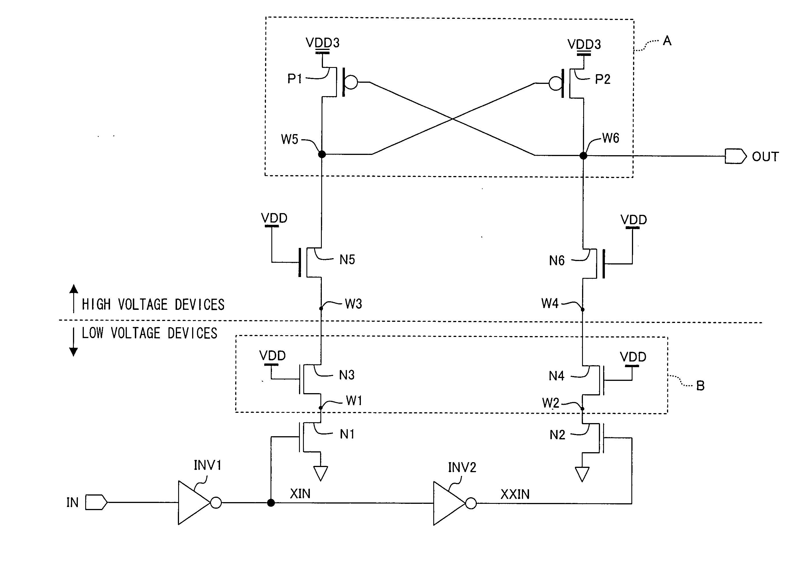
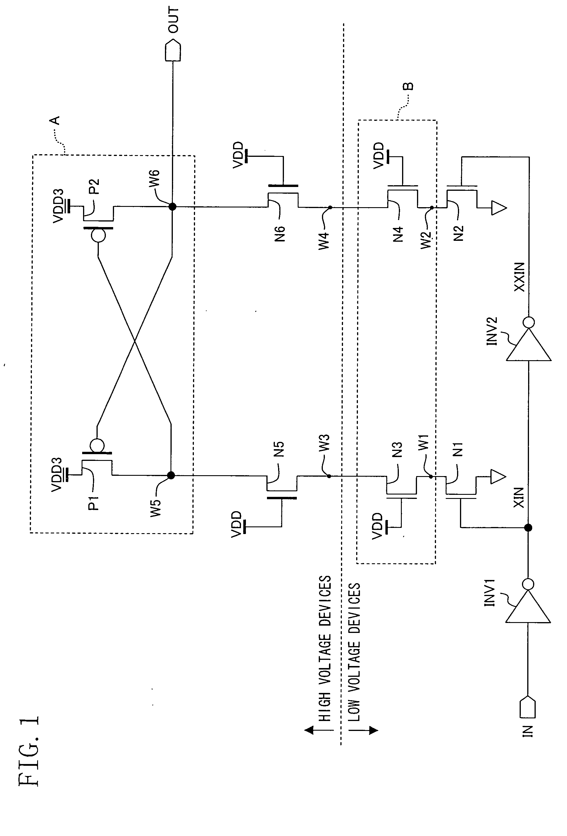
[0076]FIG. 1 is a view illustrating the specific configuration of a level shift circuit in accordance with this embodiment.

[0077] In FIG. 1, the reference mark IN denotes a signal input terminal, the reference mark INV1 denotes an inverter for inverting a signal input to the input terminal IN, and the reference mark INV2 denotes an inverter which inverts a signal output from the inverter INV1. The inverters INV1 and INV2 operate at a voltage of 1.5 V, for example, supplied from a low-voltage supply VDD.

[0078] In FIG. 1, the reference marks N1 and N2 denote N-type low-voltage transistors which receive a pair of complementary signals and are capable of withstanding only low voltage (which will be hereinafter refereed to as “N-type complementary-signal-receiving low-voltage transistors.) The N-type complementary-signal-receiving low-voltage transistors N1 and N2 have their respective sources grounded. A signal XIN (which is one of first and second signals serving as the complementary...

first modified example

of the First Embodiment

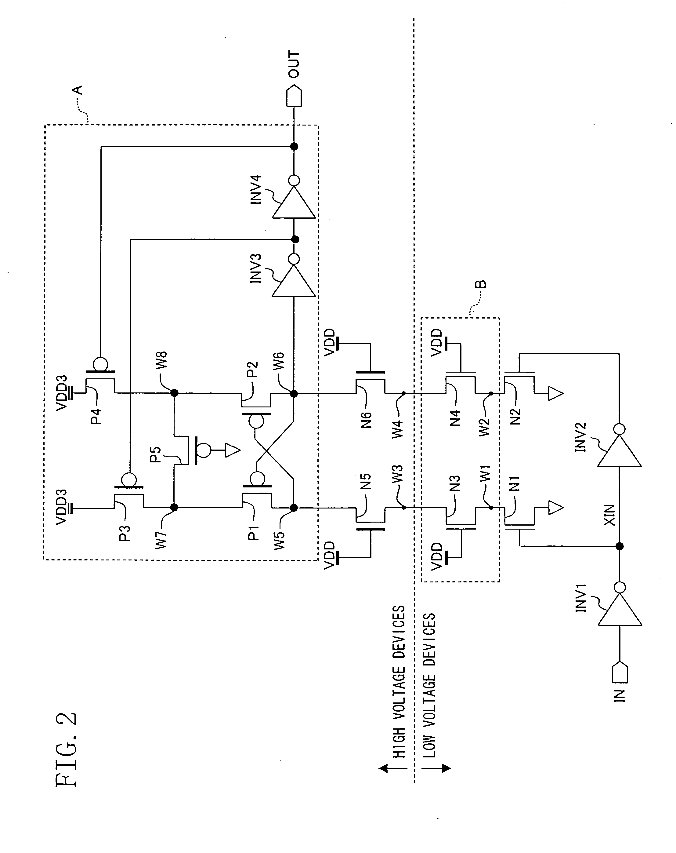
[0094]FIG. 2 illustrates a first modified example of the first embodiment.

[0095] This modified example is obtained by making modifications to the internal configuration of the power supply circuit A of the first embodiment. More specifically, in the power supply circuit A shown in FIG. 2, the reference marks P1 and P2 denote a pair of P-type transistors. The sources of the P-type transistors P1 and P2 are connected to a high-voltage supply VDD3, while the gate of each P-type transistor is cross-coupled to the drain of the other. And their respective drains are connected to the drains of N-type transistors N5 and N6. The connecting point, at which the P-type transistor (i.e., a first P-type transistor) P1 and the N-type transistor N5 are connected together, is a fifth node W5, and the connecting point, at which the other P-type transistor (i.e., a second P-type transistor) P2 and the N-type transistor N6 are connected together, is a sixth node W6.

[0096] The r...

second modified example

of the First Embodiment

[0098]FIG. 3 illustrates a second modified example of the first embodiment.

[0099] This modified example is obtained by making other modifications to the internal configuration of the power supply circuit A of the first embodiment.

[0100] More specifically, the power supply circuit A of FIG. 3 includes a precharge circuit composed of: a supply circuit consisting of a pair of P-type transistors P6 and P7; a disconnecting circuit consisting of a pair of N-type transistors N7 and N8; and a P-type transistor P8 operating as a resistor. The P-type transistor P6 has its source connected to a high-voltage supply VDD3 and its drain to a fifth node W11. The other P-type transistor P7 has its source connected to the high-voltage supply VDD3 and its drain to a sixth node W12. In the precharge circuit shown in FIG. 3, the N-type transistor N7 is disposed between the fifth node W11 and an N-type transistor N5, while the other N-type transistor N8 is disposed between the si...


PUM


Abstract

In a level shift circuit, the threshold voltage of N-type high-voltage transistors, to whose gates the voltage of a low-voltage supply VDD is applied, is set low. An input signal IN powered by the low-voltage supply VDD is input to the gate of an N-type transistor by way of an inverter. Therefore, even if the potentials at nodes W3 and W4 exceed the voltage of the low-voltage supply VDD, reverse current flow from the nodes W3 and W4 via parasitic diodes within the inverters into the low-voltage supply VDD is prevented. A protection circuit, composed of N-type transistor whose respective gates are fixed to the low-voltage supply VDD, is disposed between the two N-type high-voltage transistors N5, N6 and two N-type low-voltage transistors N1, N2 for receiving the complementary signals IN and XIN, thereby preventing the breakdown of those N-type complementary-signal-receiving transistors.

Description

CROSS-REFERENCE TO RELATED APPLICATIONS [0001] This non-provisional application claims priority under 35 U.S.C.§119(a) on Patent Applications No. 2003-421155 filed in Japan on Dec. 18, 2003 and No. 2004-330249 filed in Japan on Nov. 15, 2004, the entire contents of which are hereby incorporated by references. BACKGROUND OF THE INVENTION [0002] The present invention relates to level shift circuits for translating logic levels, and more particularly relates to level shift circuits configured to operate at low voltage with reduced power dissipation. [0003] A conventional level shift circuit disclosed in Japanese Laid-Open Publication No. 4-40798 has been known. FIG. 14 illustrates the configuration of the conventional level shift circuit. [0004] The level shift circuit shown in FIG. 14 includes two N-type transistors N5 and N6, two cross-coupled P-type transistors P1 and P2, and first and second inverters INV1 and INV2. Each P-type transistor P1 or P2 has its gate connected to the drai...

Claims


Application Information

Patent Timeline
Patent Type & Authority Applications(United States)
IPC IPC(8): H03K3/356H03K17/10
CPCH03K17/102H03K3/356113
Inventor MAEDE, MASATONOJIRI, NAOKIGION, MASAHIROKINUYAMA, SHINJIMATSUOKA, DAISUKEUSAMI, SHIRO
Owner PANASONIC CORP
Why Eureka
Try Eureka