Method for inspection of a wafer
- Summary
- Abstract
- Description
- Claims
- Application Information
AI Technical Summary
Benefits of technology
Problems solved by technology
Method used
Image

Examples
Embodiment Construction
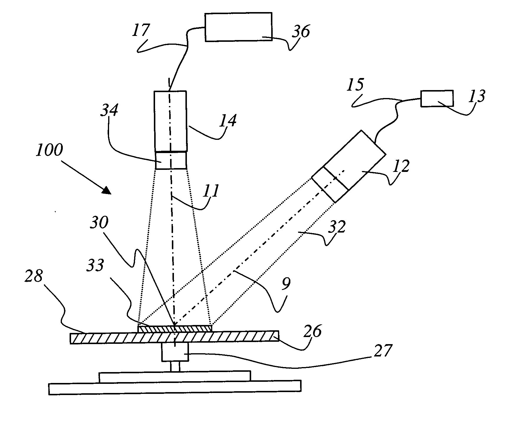
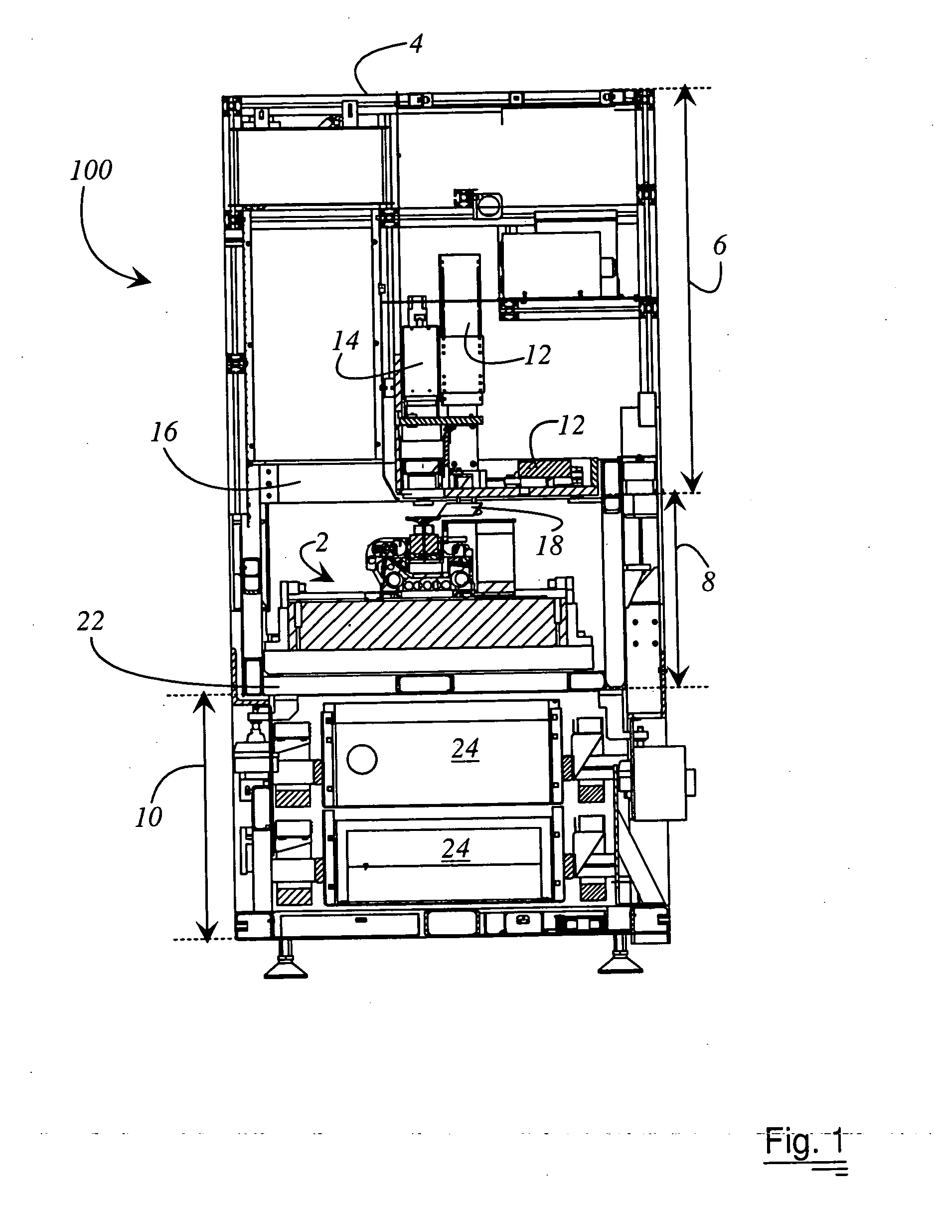
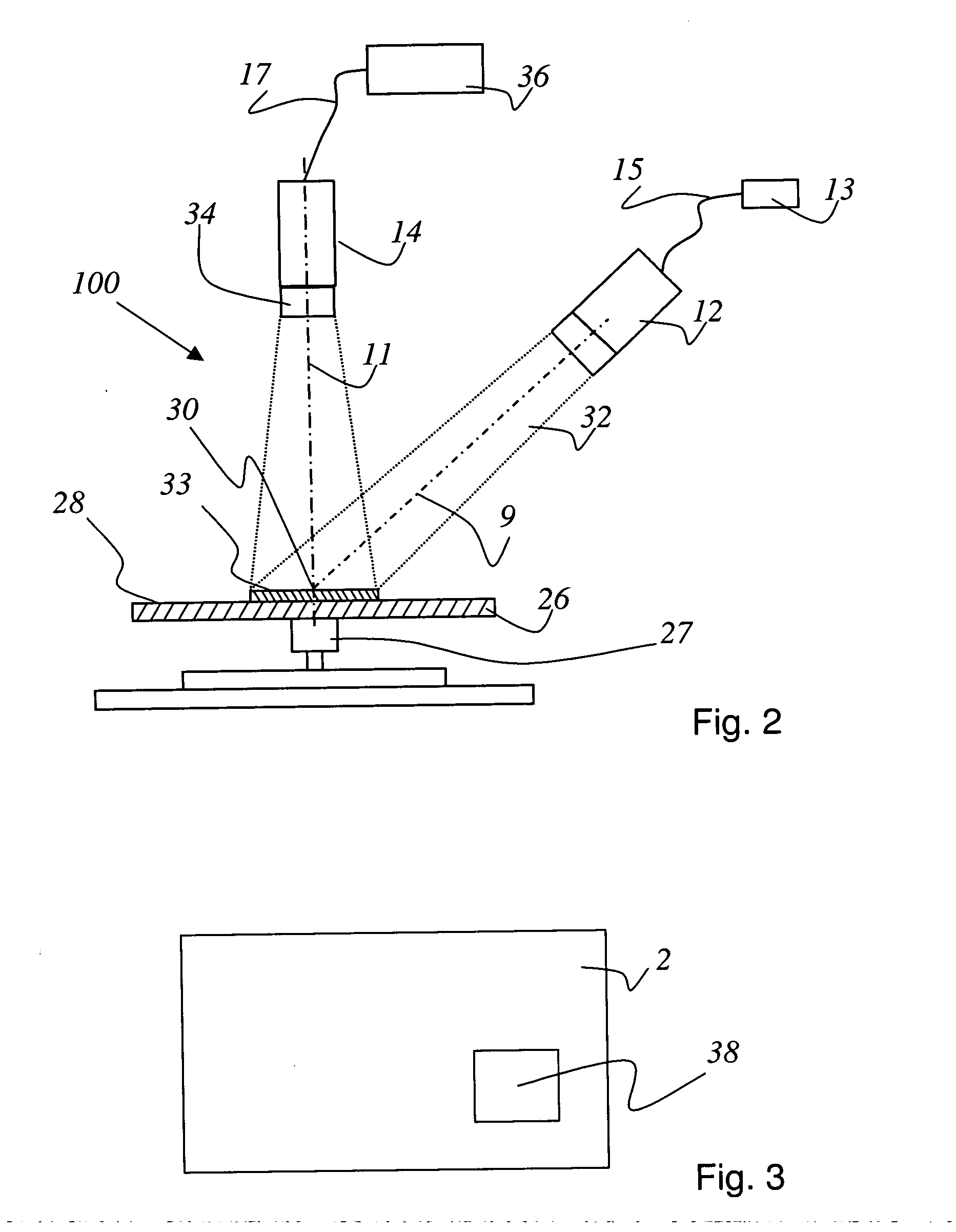
[0028]FIG. 1 depicts an overall system 100 for the inspection of a wafer 26. System 100 is enclosed by a housing 4 and is subdivided into a first segment 6, a second segment 8, and a third segment 10. Housing 4 is closed off on all external surfaces by walls (not depicted), so that specific climatic or clean-room conditions are present in the interior of housing 4. Housed in first segment 6 of housing 4 are substantially several illumination devices 12 and at least one image acquisition device 14. Image acquisition device 14 is usually a CCD camera. First segment 6 is separated from second segment 8 by a mounting plate 16. The light of illumination devices 12 is directed via optical means 18 through mounting plate 16 onto the surface of the wafer to be inspected. Stage 2, which is movable in the X direction and Y direction, is provided in second segment 8. Stage 2 is mounted on a separating plate 22 that separates second and third segments 8 and 10 from one another. Third segment 10...
PUM
 Abstract
Description
Claims
Application Information
 - Generate Ideas
- Intellectual Property
- Life Sciences
- Materials
- Tech Scout
- Unparalleled Data Quality
- Higher Quality Content
- 60% Fewer Hallucinations
Browse by: Latest US Patents, China's latest patents, Technical Efficacy Thesaurus, Application Domain, Technology Topic, Popular Technical Reports.
© 2025 PatSnap. All rights reserved.Legal|Privacy policy|Modern Slavery Act Transparency Statement|Sitemap|About US| Contact US: help@patsnap.com