Printed circuits on shrink film

a technology of printed circuits and shrink films, applied in the field of printed circuits on shrink films, can solve the problems of inability to produce feature sizes smaller than 50-70 micrometers, non-digital approaches that are too expensive and therefore impractical, etc., and achieve the effect of quick and inexpensive production

Inactive Publication Date: 2005-06-23
3M INNOVATIVE PROPERTIES CO
View PDF10 Cites 24 Cited by
  • Summary
  • Abstract
  • Description
  • Claims
  • Application Information

AI Technical Summary

Benefits of technology

[0004] Materials and methods of the present invention generally are useful in the manufacture of fine resolution circuitry, typically, quickly, inexpensively, and without the need for custom hard tooling.

Problems solved by technology

For rapid prototyping, custom circuitry, or short run manufacturing, these non-digital approaches typically become too expensive and therefore impractical.
However, existing digital methods generally fail to produce feature sizes smaller than 50-70 micrometers.

Method used


Image

  • Printed circuits on shrink film
  • Printed circuits on shrink film
  • Printed circuits on shrink film

Examples


examples

[0044] These examples are merely for illustrative purposes only and are not meant to be limiting on the scope of the appended claims. All parts, percentages, ratios, etc. in the examples and the rest of the specification are by weight, unless noted otherwise. Unless otherwise noted, all reagents used in the examples were obtained, or are available, from general chemical suppliers such as, for example, Sigma-Aldrich Company, Saint Louis, Mo., or may be synthesized by conventional methods.

[0045] n-Tetradecane used in the examples was obtained from Avocado Research Chemicals, Ltd.; Lancashire, England.

TABLE OF ABBREVIATIONSAbbre-viationDescriptionSilverA silver nanoparticulate ink from Harima Chemical Company;Ink 1Tokodai, Japan, used as received as a stable dispersion of ˜58percent by weight 7 nanometer silver particles, surface treatedwith decanol and dispersed in n-tetradecane, as described inJP200266002A.SilverSame as Silver Ink-1 but diluted to 27.5 percent by weight silverInk ...

examples 1-6

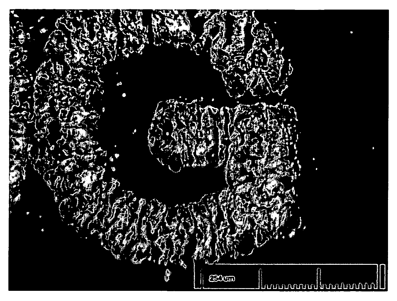
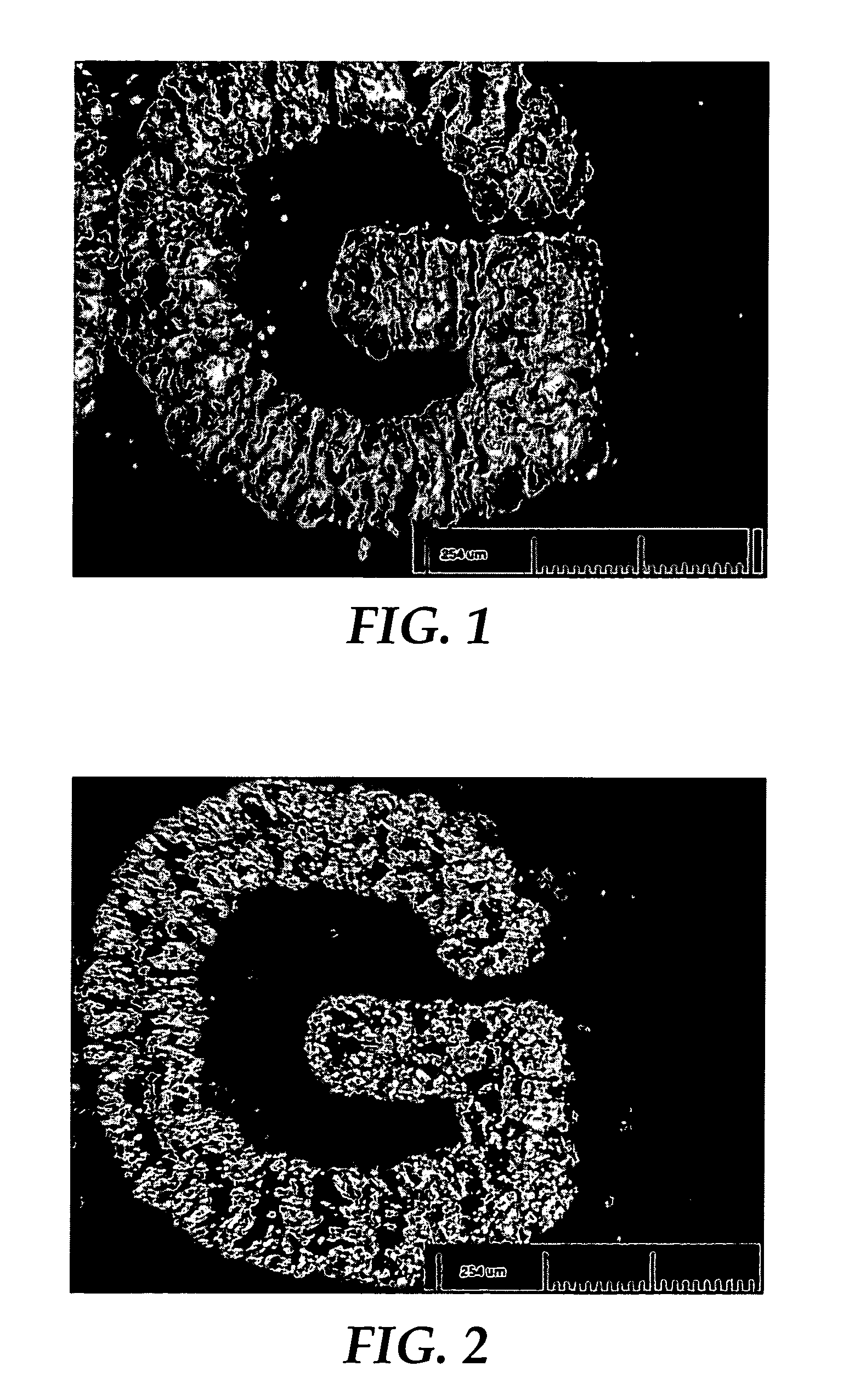
[0047] Silver Ink-1 (Example 1-3) and Silver Ink-2 (Example 4-6) were printed at 317×295 dots per inch (dpi) resolution using a piezo inkjet print head obtained under the trade designation “XJ128-200” from Xaar PLC, Cambridge, United Kingdom, and mounted on an XY translational stage. The print head was driven at 1250 Hz and 35 Volts. Samples were printed onto Shrink Films 1-3 in a variety of patterns with varying feature sizes and dried in 100° C. oven for 10 minutes.

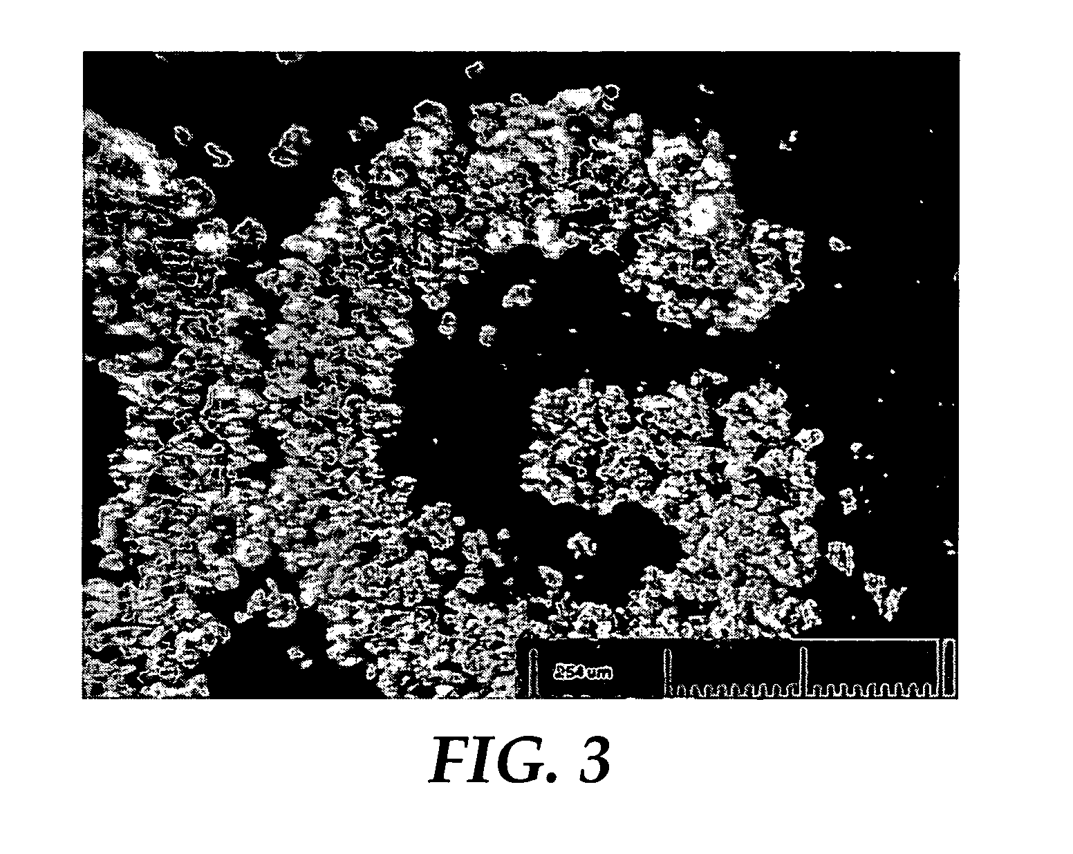
[0048] The three printed shrink films were shrunk by placing the printed shrink films between two flat polytetrafluoroethylene-coated mesh screens. The screens were then placed into a 170° C. oven for 45 seconds, after which no further relaxation in the shrink films was observed, resulting in an overall area reduction of approximately 25-fold. The screens holding the shrunk film samples were then removed from the oven and allowed to cool to room temperature, and the shrunk film was removed from in between the screens. ...


PUM

PropertyMeasurementUnit
sizeaaaaaaaaaa
weight percentaaaaaaaaaa
sizesaaaaaaaaaa

Abstract

Methods of creating fine featured circuits by printing a circuit trace onto polymer shrink films or other biaxially-oriented polymer films are disclosed. The shrink films are heated and shrunk after printing, annealing the circuit trace to form conductive features. Compositions suitable for printing onto the films and articles made using the method and composition are also disclosed.

Description

BACKGROUND [0001] The ability to manufacture electronic circuitry with increasingly fine features has become important for many electronic devices. Increasing the resolution of electronic circuitry typically enables a reduction in the total size of the circuitry. Fine resolution circuitry is generally produced based on non-digital technologies, such as photolithography, micro-contact printing, and vapor deposition, all of which involve the use of hard tooling in some form. [0002] For rapid prototyping, custom circuitry, or short run manufacturing, these non-digital approaches typically become too expensive and therefore impractical. These customized applications would benefit from a digital methodology that allows for rapid modifications of designs. However, existing digital methods generally fail to produce feature sizes smaller than 50-70 micrometers. SUMMARY OF THE INVENTION [0003] In certain implementations the present invention includes a method of forming a substrate containin...

Claims


Application Information

Patent Timeline
Patent Type & Authority Applications(United States)
IPC IPC(8): H05K3/10H05K3/12H05K3/22
CPCH05K3/105H05K3/12H05K3/125H05K3/22H05K2201/0125Y10T428/2857H05K2201/0329H05K2203/013H05K2203/1105Y10S428/901Y10T428/24917H05K2201/0257Y10T428/31504Y10T428/31678Y10T428/31938
Inventor VOSS-KEHL, JESSICA L.HALVERSON, KURT J.YLITALO, CAROLINE M.LEHMANN, MATTHEW R.BOTZET, STEVEN J.
Owner 3M INNOVATIVE PROPERTIES CO
Why Eureka
Try Eureka