Semiconductor device with modified mobility and thin film transistor having the same

a thin film transistor and mobility technology, applied in the direction of semiconductors, semiconductor devices, electrical appliances, etc., can solve the problems of deteriorating the quality of display devices, improving the uniformity of polycrystalline materials, etc., and achieve the effect of improving the uniformity of silicon crystalline materials and high-quality semiconductors

Inactive Publication Date: 2005-06-30
SAMSUNG ELECTRONICS CO LTD
View PDF11 Cites 15 Cited by
  • Summary
  • Abstract
  • Description
  • Claims
  • Application Information

AI Technical Summary

Benefits of technology

[0009] The present invention provides a high-quality semiconductor device formed by improving the uniformity of silicon crystalline with an array structure and a TFT having the high-quality semiconductor device.

Problems solved by technology

However, the improvement of the uniformity of polycrystalline is a problem to be still solved and a subject to be presently studied.
The mobility deviation of this degree deteriorates the quality of a display device.

Method used


Image

  • Semiconductor device with modified mobility and thin film transistor having the same
  • Semiconductor device with modified mobility and thin film transistor having the same
  • Semiconductor device with modified mobility and thin film transistor having the same

Examples


Embodiment Construction

[0026] A Si semiconductor device, according to the present invention, and a TFT having the Si semiconductor device will be described in detail with reference to the attached drawings.

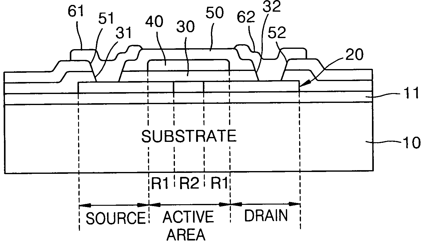
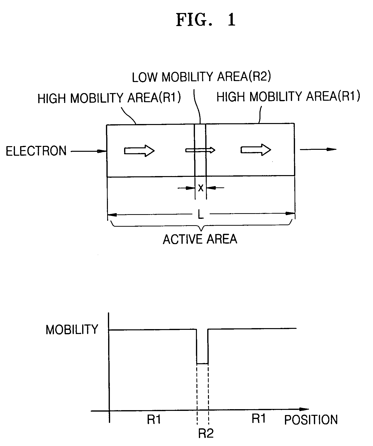
[0027]FIG. 1 is a view for explaining a technical concept of a Si semiconductor device, according to the present invention. As shown in FIG. 1, the Si semiconductor device of the present invention has a structure in which high and low mobility areas R1 and R2 are formed in an active area that is an electron mobility channel having a predetermined length L. In other words, a channel of a Si semiconductor device includes an active area through which electrons flow. The active area includes a high mobility area which is formed of poly-Si having high mobility and a low mobility area which is formed of amorphous silicon (a-Si) having a predetermined length x. Here, the Si semiconductor device according to an embodiment of the present invention may be the above-described channel or a device including the cha...


PUM


Abstract

Provided are a semiconductor device including an active area which is defined as high and low mobility areas and a thin film transistor having the semiconductor device. The mobility of the active area can be lowered to a level enough to satisfy the requirement of the semiconductor device. The lowering of the mobility of the active area can contribute to reducing mobility deviation between semiconductor devices. As a result, the quality of a flat panel display adopting a large-scale semiconductor device can be greatly improved.

Description

[0001] Priority is claimed to Korean Patent Application No. 10-2003-0100494, filed on Dec. 30, 2003, in the Korean Intellectual Property Office, the disclosure of which is incorporated herein in its entirety by reference. BACKGROUND OF THE INVENTION [0002] 1. Field of the Invention [0003] The present invention relates to a polycrystalline silicon device and a thin film transistor (TFT) having the same, and more particularly, to a polycrystalline silicon device with uniform mobility and a TFT having the same. [0004] 2. Description of the Related Art [0005] Polycrystalline silicon (poly-Si) has higher mobility and better light stability than amorphous silicon. Such poly-Si is used widely in various application fields, particularly, in TFTs or memory devices. A poly-Si TFT is used, for example, as a switching device of a display. Examples of a display device using an active element such as a TFT include a TFT-liquid crystal display (LCD), a TFT-organic light emitting diode (OLED), or t...

Claims


Application Information

Patent Timeline
Patent Type & Authority Applications(United States)
IPC IPC(8): H01L21/20H01L21/336H01L21/77H01L29/04H01L29/10H01L29/786
CPCH01L21/2026H01L27/1285H01L27/1296H01L29/04H01L29/78696H01L29/6675H01L29/78663H01L29/78672H01L29/1029H01L21/02686H01L21/02381H01L21/02488H01L21/02678H01L21/02532H01L29/786
Inventor KWON, JANG-YEONNOGUCHI, TAKASHIPARK, YOUNG-SOOKIM, DO-YOUNG
Owner SAMSUNG ELECTRONICS CO LTD
Why Eureka
Try Eureka